TL F 9508
54F74F258A
Quad
2-Input
Multiplexer
with
TRI-STATE
Outputs
November 1994
54F 74F258A
Quad 2-Input Multiplexer with TRI-STATE
Outputs
General Description
The 'F258A is a quad 2-input multiplexer with TRI-STATE
outputs Four bits of data from two sources can be selected
using a common data select input The four outputs present
the selected data in the complement (inverted) form The
outputs may be switched to a high impedance state with a
HIGH on the common Output Enable (OE) input allowing
the outputs to interface directly with bus-oriented systems
Features
Y
Multiplexer expansion by tying outputs together
Y
Inverting TRI-STATE outputs
Y
Guaranteed 4000V minimum ESD protection
Commercial
Military
Package
Package Description
Number
74F258APC
N16E
16-Lead (0 300 Wide) Molded Dual-In-Line
54F258ADM (Note 2)
J16A
16-Lead Ceramic Dual-In-Line
74F258ASC (Note 1)
M16A
16-Lead (0 150 Wide) Molded Small Outline JEDEC
74F258ASJ (Note 1)
M16D
16-Lead (0 300 Wide) Molded Small Outline EIAJ
54F258AFM (Note 2)
W16A
16-Lead Cerpack
54F258ALL (Note 2)
E20A
20-Lead Ceramic Leadless Chip Carrier Type C
Note 1
Devices also available in 13
reel Use suffix
e
SCX and SJX
Note 2
Military grade device with environmental and burn-in processing Use suffix
e
DMQB FMQB and LMQB
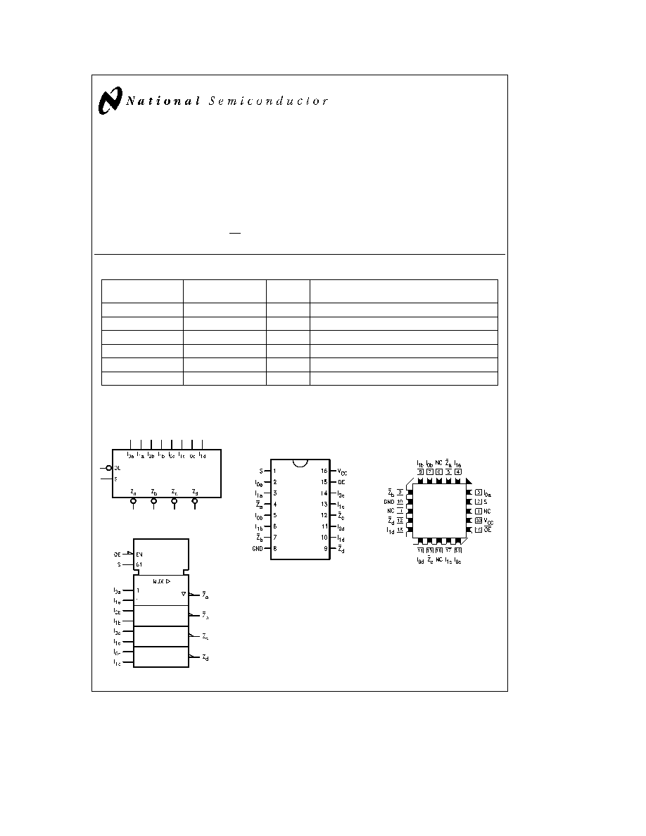
Logic Symbols
Connection Diagrams
TL F 9508 � 3
IEEE IEC
TL F 9508 � 5
Pin Assignment
for DIP SOIC and Flatpak
TL F 9508 � 1
Pin Assignment
for LCC
TL F 9508 � 2
TRI-STATE
is a registered trademark of National Semiconductor Corporation
C1995 National Semiconductor Corporation
RRD-B30M75 Printed in U S A
Unit Loading Fan Out
54F 74F
Pin Names
Description
U L
Input I
IH
I
IL
HIGH LOW
Output I
OH
I
OL
S
Common Data Select Input
1 0 1 0
20 mA
b
0 6 mA
OE
TRI-STATE Output Enable Input (Active LOW)
1 0 1 0
20 mA
b
0 6 mA
I
0a
� I
0d
Data Inputs from Source 0
1 0 1 0
20 mA
b
0 6 mA
I
1a
� I
1d
Data Inputs from Source 1
1 0 1 0
20 mA
b
0 6 mA
Z
a
� Z
d
TRI-STATE Inverting Data Outputs
150 40 (33 3)
b
3 mA 24 mA (20 mA)
Functional Description
The 'F258A is a quad 2-input multiplexer with TRI-STATE
outputs It selects four bits of data from two sources under
control of a common Select input (S) When the Select input
is LOW the I
0x
inputs are selected and when Select is
HIGH the I
1x
inputs are selected The data on the selected
inputs appears at the outputs in inverted form The 'F258A
is the logic implementation of a 4-pole 2-position switch
where the position of the switch is determined by the logic
levels supplied to the Select input The logic equation for
the outputs is shown below
Z
n
e
OE
(I
1n
S
a
I
0n
S)
When the Output Enable input (OE) is HIGH the outputs are
forced to a high impedance OFF state If the outputs of the
TRI-STATE devices are tied together all but one device
must be in the high impedance state to avoid high currents
that would exceed the maximum ratings Designers should
ensure that Output Enable signals to TRI-STATE devices
whose outputs are tied together are designed so there is no
overlap
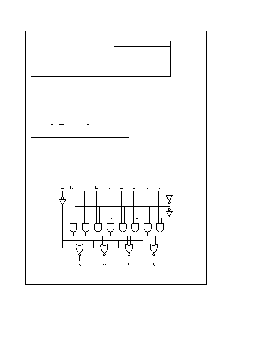
Truth Table
Output
Select
Data
Output
Enable
Input
Inputs
OE
S
I
0
I
1
Z
H
e
HIGH Voltage Level
L
e
LOW Voltage Level
H
X
X
X
Z
X
e
Immaterial
L
H
X
L
H
Z
e
High Impedance
L
H
X
H
L
L
L
L
X
H
L
L
H
X
L
Logic Diagram
TL F 9508 � 4
Please note that this diagram is provided only for the understanding of logic operations and should not be used to estimate propagation delays
2

Absolute Maximum Ratings
(Note 1)
If Military Aerospace specified devices are required
please contact the National Semiconductor Sales
Office Distributors for availability and specifications
Storage Temperature
b
65 C to
a
150 C
Ambient Temperature under Bias
b
55 C to
a
125 C
Junction Temperature under Bias
b
55 C to
a
175 C
Plastic
b
55 C to
a
150 C
V
CC
Pin Potential to
Ground Pin
b
0 5V to
a
7 0V
Input Voltage (Note 2)
b
0 5V to
a
7 0V
Input Current (Note 2)
b
30 mA to
a
5 0 mA
Voltage Applied to Output
in HIGH State (with V
CC
e
0V)
Standard Output
b
0 5V to V
CC
TRI-STATE Output
b
0 5V to
a
5 5V
Current Applied to Output
in LOW State (Max)
twice the rated I
OL
(mA)
ESD Last Passing Voltage (Min)
4000V
Note 1
Absolute maximum ratings are values beyond which the device may
be damaged or have its useful life impaired Functional operation under
these conditions is not implied
Note 2
Either voltage limit or current limit is sufficient to protect inputs
Recommended Operating
Conditions
Free Air Ambient Temperature
Military
b
55 C to
a
125 C
Commercial
0 C to
a
70 C
Supply Voltage
Military
a
4 5V to
a
5 5V
Commercial
a
4 5V to
a
5 5V
DC Electrical Characteristics
Symbol
Parameter
54F 74F
Units
V
CC
Conditions
Min
Typ
Max
V
IH
Input HIGH Voltage
2 0
V
Recognized as a HIGH Signal
V
IL
Input LOW Voltage
0 8
V
Recognized as a LOW Signal
V
CD
Input Clamp Diode Voltage
b
1 2
V
Min
I
IN
e b
18 mA
V
OH
Output HIGH
54F 10% V
CC
2 5
I
OH
e b
1 mA
Voltage
54F 10% V
CC
2 4
I
OH
e b
3 mA
74F 10% V
CC
2 5
V
Min
I
OH
e b
1 mA
74F 10% V
CC
2 4
I
OH
e b
3 mA
74F 5% V
CC
2 7
I
OH
e b
1 mA
74F 5% V
CC
2 7
I
OH
e b
3 mA
V
OL
Output LOW
54F 10% V
CC
0 5
V
Min
I
OL
e
20 mA
Voltage
74F 10% V
CC
0 5
I
OL
e
24 mA
I
IH
Input HIGH
54F
20 0
m
A
Max
V
IN
e
2 7V
Current
74F
5 0
I
BVI
Input HIGH Current
54F
100
m
A
Max
V
IN
e
7 0V
Breakdown Test
74F
7 0
I
CEX
Output HIGH
54F
250
m
A
Max
V
OUT
e
V
CC
Leakage Current
74F
50
V
ID
Input Leakage
74F
4 75
V
0 0
I
ID
e
1 9 mA
Test
All Other Pins Grounded
I
OD
Output Leakage
74F
3 75
m
A
0 0
V
IOD
e
150 mV
Circuit Current
All Other Pins Grounded
I
IL
Input LOW Current
b
0 6
mA
Max
V
IN
e
0 5V
I
OZH
Output Leakage Current
50
m
A
Max
V
OUT
e
2 7V
I
OZL
Output Leakage Current
b
50
m
A
Max
V
OUT
e
0 5V
I
OS
Output Short-Circuit Current
b
60
b
150
mA
Max
V
OUT
e
0V
I
ZZ
Bus Drainage Test
500
m
A
0 0V
V
OUT
e
V
CC
I
CCH
Power Supply Current
6 2
9 5
mA
Max
V
O
e
HIGH
I
CCL
Power Supply Current
15 1
23
mA
Max
V
O
e
LOW
I
CCZ
Power Supply Current
11 3
17
mA
Max
V
O
e
HIGH Z
3
AC Electrical Characteristics
74F
54F
74F
T
A
e a
25 C
T
A
V
CC
e
Mil
T
A
V
CC
e
Com
Symbol
Parameter
V
CC
e a
5 0V
C
L
e
50 pF
C
L
e
50 pF
Units
C
L
e
50 pF
Min
Typ
Max
Min
Max
Min
Max
t
PLH
Propagation Delay
2 5
5 3
2 0
7 5
2 0
6 0
ns
t
PHL
I
n
to Z
n
1 0
4 0
1 0
6 0
1 0
5 0
t
PLH
Propagation Delay
3 0
7 5
3 0
9 5
3 0
8 5
ns
t
PHL
S to Z
n
2 5
7 0
2 5
9 0
2 5
8 0
t
PZH
Output Enable Time
2 0
6 0
2 0
8 0
2 0
7 0
t
PZL
2 5
7 0
2 5
9 0
2 5
8 0
t
PHZ
Output Disable Time
2 0
6 0
1 5
7 0
2 0
7 0
ns
t
PLZ
2 0
6 0
2 0
8 5
2 0
7 0
4
Ordering Information
The device number is used to form part of a simplified purchasing code where the package type and temperature range are
defined as follows
74F
258A
S
C
X
Temperature Range Family
Special Variations
74F
e
Commercial
X
e
Devices shipped in 13 reels
54F
e
Military
QB
e
Military grade with
environmental and burn-in
Device Type
processing shipped in tubes
Package Code
Temperature Range
P
e
Plastic DIP
C
e
Commercial (0 C to
a
70 C)
D
e
Ceramic DIP
M
e
Military (
b
55 C to
a
125 C)
F
e
Flatpak
L
e
Leadless Ceramic Chip Carrier (LCC)
S
e
Small Outline SOIC JEDEC
SJ
e
Small Outline SOIC EIAJ
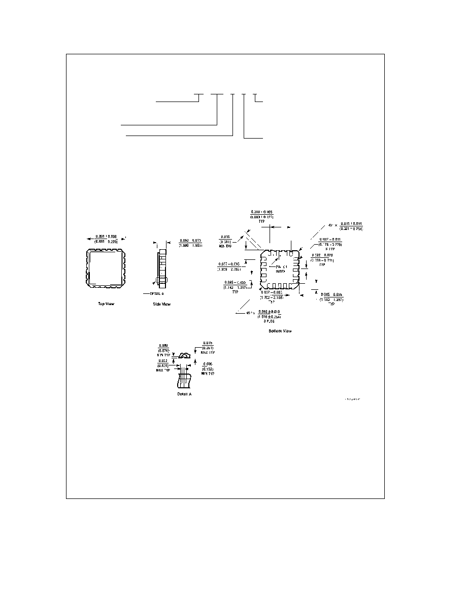
Physical Dimensions
inches (millimeters)
20-Lead Ceramic Leadless Chip Carrier (L)
NS Package Number E20A
5