 | –≠–ª–µ–∫—Ç—Ä–æ–Ω–Ω—ã–π –∫–æ–º–ø–æ–Ω–µ–Ω—Ç: ADC0820 | –°–∫–∞—á–∞—Ç—å:  PDF PDF  ZIP ZIP |
ADC0820
8-Bit High Speed µP Compatible A/D Converter with
Track/Hold Function
General Description
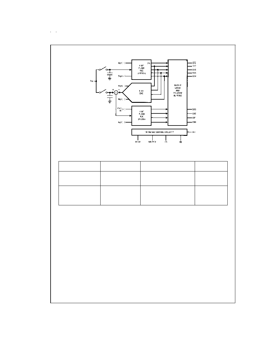
By using a half-flash conversion technique, the 8-bit
ADC0820 CMOS A/D offers a 1.5 µs conversion time and
dissipates only 75 mW of power. The half-flash technique
consists of 32 comparators, a most significant 4-bit ADC and
a least significant 4-bit ADC.
The input to the ADC0820 is tracked and held by the input
sampling circuitry eliminating the need for an external
sample-and-hold for signals moving at less than 100 mV/µs.
For ease of interface to microprocessors, the ADC0820 has
been designed to appear as a memory location or I/O port
without the need for external interfacing logic.
Key Specifications
n
Resolution
8 Bits
n
Conversion Time
2.5 µs Max (RD Mode)
1.5 µs Max (WR-RD Mode)
n
Low Power
75 mW Max
n
Total Unadjusted
Error
±
1
/
2
LSB and
±
1 LSB
Features
n
Built-in track-and-hold function
n
No missing codes
n
No external clocking
n
Single supply -- 5 V
DC
n
Easy interface to all microprocessors, or operates
stand-alone
n
Latched TRI-STATE
Æ
output
n
Logic inputs and outputs meet both MOS and T
2
L
voltage level specifications
n
Operates ratiometrically or with any reference value
equal to or less than V
CC
n
0V to 5V analog input voltage range with single 5V
supply
n
No zero or full-scale adjust required
n
Overflow output available for cascading
n
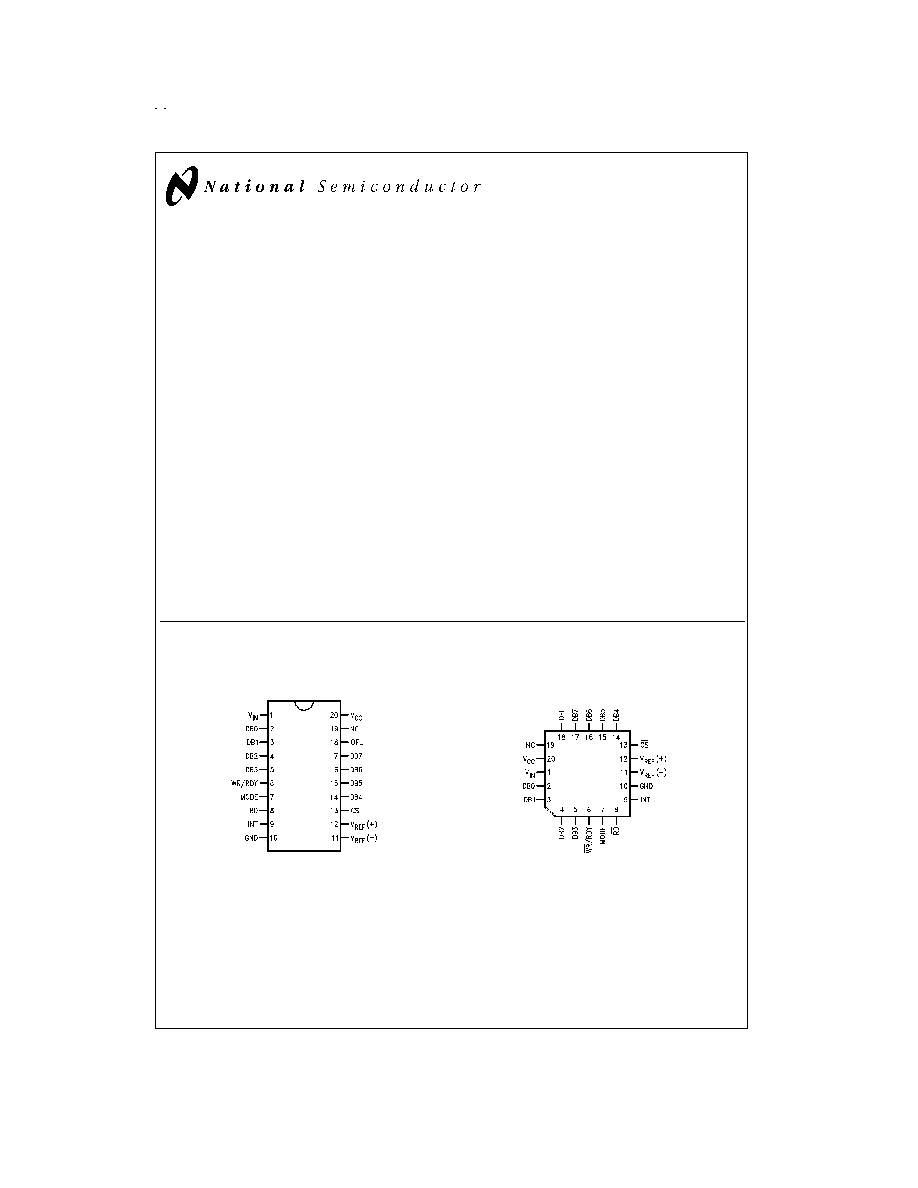
0.3" standard width 20-pin DIP
n
20-pin molded chip carrier package
n
20-pin small outline package
n
20-pin shrink small outline package (SSOP)
Connection and Functional Diagrams
TRI-STATE
Æ
is a registered trademark of National Semiconductor Corporation.
Dual-In-Line, Small Outline
and SSOP Packages
DS005501-1
Top View
Molded Chip Carrier
Package
DS005501-33
June 1999
ADC0820
8-Bit
High
Speed
µP
Compatible
A/D
Converter
with
T
rack/Hold
Function
© 1999 National Semiconductor Corporation
DS005501
www.national.com
Connection and Functional Diagrams
(Continued)
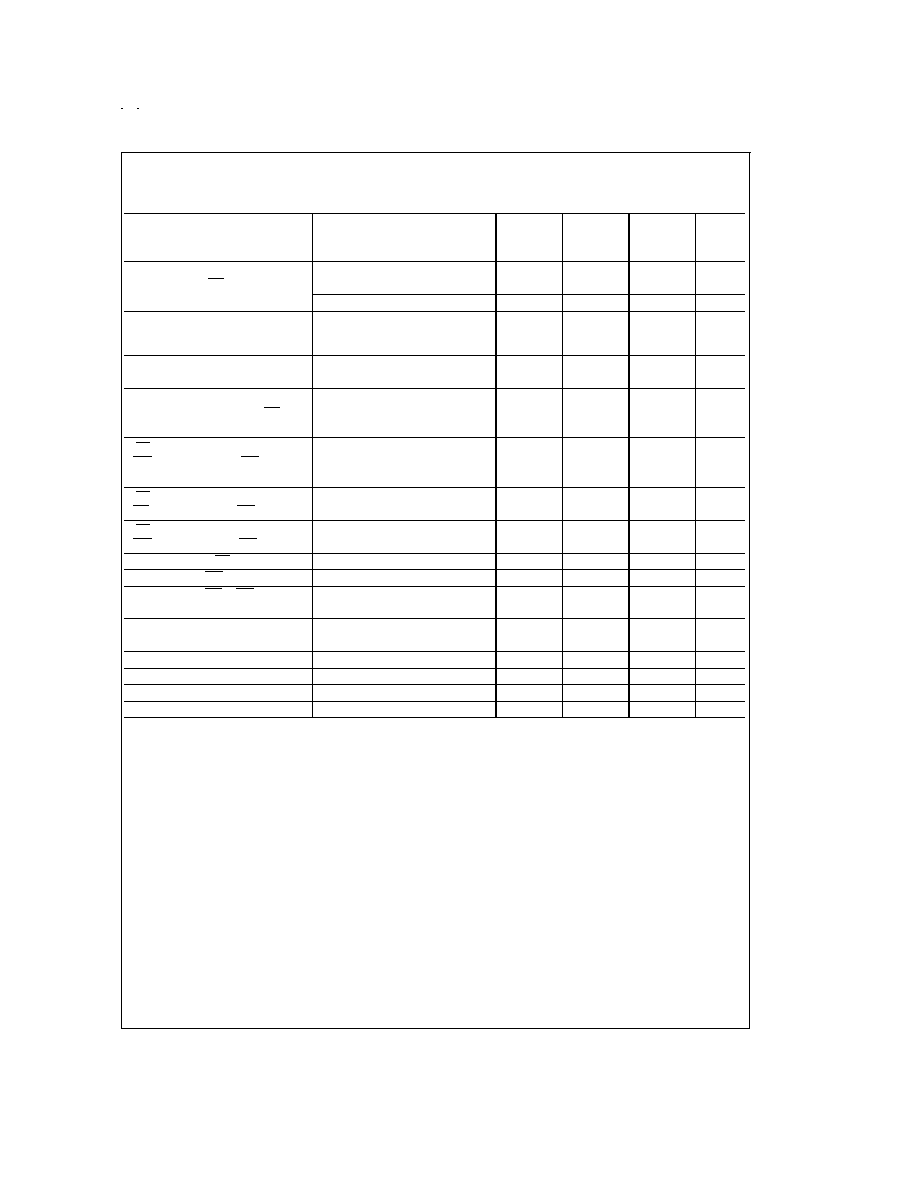
Ordering Information
Part Number
Total
Package
Temperature
Unadjusted Error
Range
ADC0820BCV
V20A -- Molded Chip Carrier
0∞C to +70∞C
ADC0820BCWM
±
1
/
2
LSB
M20B -- Wide Body Small Outline
0∞C to +70∞C
ADC0820BCN
N20A -- Molded DIP
0∞C to +70∞C
ADC0820CCJ
±
1 LSB
J20A -- Cerdip
-40∞C to +85∞C
ADC0820CCWM
M20B -- Wide Body Small Outline
0∞C to +70∞C
ADC0820CIWM
M20B -- Wide Body Small Outline
-40∞C to +85∞C
ADC0820CCN
N20A -- Molded DIP
0∞C to +70∞C
DS005501-2
FIGURE 1.
www.national.com
2
Absolute Maximum Ratings
(Notes 1, 2)
If Military/Aerospace specified devices are required,
please contact the National Semiconductor Sales Office/
Distributors for availability and specifications.
Supply Voltage (V
CC
)
10V
Logic Control Inputs
-0.2V to V
CC
+0.2V
Voltage at Other Inputs and Output
-0.2V to V
CC
+0.2V
Storage Temperature Range
-65∞C to +150∞C
Package Dissipation at T
A
= 25∞C
875 mW
Input Current at Any Pin (Note 5)
1 mA
Package Input Current (Note 5)
4 mA
ESD Susceptability (Note 9)
1200V
Lead Temp. (Soldering, 10 sec.)
Dual-In-Line Package (plastic)
260∞C
Dual-In-Line Package (ceramic)
300∞C
Surface Mount Package
Vapor Phase (60 sec.)
215∞C
Infrared (15 sec.)
220∞C
Operating Ratings
(Notes 1, 2)
Temperature Range
T
MIN
T
A
T
MAX
ADC0820CCJ
-40∞C
T
A
+85∞C
ADC0820CIWM
-40∞C
T
A
+85∞C
ADC0820BCN, ADC0820CCN
0∞C
T
A
70∞C
ADC0820BCV
0∞C
T
A
70∞C
ADC0820BCWM, ADC0820CCWM
0∞C
T
A
70∞C
V
CC
Range
4.5V to 8V
Converter Characteristics
The following specifications apply for RD mode (pin 7=0), V
CC
=5V, V
REF
(+)=5V,and V
REF
(-)=GND unless otherwise speci-
fied. Boldface limits apply from T
MIN
to T
MAX
; all other limits T
A
=T
j
=25∞C.
Parameter
Conditions
ADC0820BCN, ADC0820CCN
Limit
Units
ADC0820CCJ
ADC0820BCV, ADC0820BCWM
ADC0820CCWM, ADC0820CIWM
Typ
Tested
Design
Typ
Tested
Design
(Note 6)
Limit
Limit
(Note 6)
Limit
Limit
(Note 7)
(Note 8)
(Note 7)
(Note 8)
Resolution
8
8
8
Bits
Total Unadjusted
ADC0820BCN, BCWM
±
1
/
2
±
1
/
2
LSB
Error
ADC0820CCJ
±
1
LSB
(Note 3)
ADC0820CCN, CCWM, CIWM,
±
1
±
1
LSB
ADC0820CCMSA
±
1
±
1
LSB
Minimum Reference
2.3
1.00
2.3
1.2
k
Resistance
Maximum Reference
2.3
6
2.3
5.3
6
k
Resistance
Maximum V
REF
(+)
V
CC
V
CC
V
CC
V
Input Voltage
Minimum V
REF
(-)
GND
GND
GND
V
Input Voltage
Minimum V
REF
(+)
V
REF
(-)
V
REF
(-)
V
REF
(-)
V
Input Voltage
Maximum V
REF
(-)
V
REF
(+)
V
REF
(+)
V
REF
(+)
V
Input Voltage
Maximum V
IN
Input
V
CC
+0.1
V
CC
+0.1
V
CC
+0.1
V
Voltage
Minimum V
IN
Input
GND-0.1
GND-0.1
GND-0.1
V
Voltage
Maximum Analog
CS =V
CC
Input Leakage
V
IN
=V
CC
3
0.3
3
µA
Current
V
IN
=GND
-3
-0.3
-3
µA
Power Supply
V
CC
=5V
±
5%
±
1/16
±
1
/
4
±
1/16
±
1
/
4
±
1
/
4
LSB
Sensitivity
www.national.com
3
DC Electrical Characteristics
The following specifications apply for V
CC
=5V, unless otherwise specified. Boldface limits apply from T
MIN
to T
MAX
; all other
limits T
A
=T
J
=25∞C.
Parameter
Conditions
ADC0820BCN, ADC0820CCN
Limit
Units
ADC0820CCJ
ADC0820BCV, ADC0820BCWM
ADC0820CCWM, ADC0820CIWM
Typ
Tested
Design
Typ
Tested
Design
(Note 6)
Limit
Limit
(Note 6)
Limit
Limit
(Note 7)
(Note 8)
(Note 7)
(Note 8)
V
IN(1)
, Logical "1"
V
CC
=5.25V
CS , WR , RD
2.0
2.0
2.0
V
Input Voltage
Mode
3.5
3.5
3.5
V
V
IN(0)
, Logical "0"
V
CC
=4.75V
CS , WR , RD
0.8
0.8
0.8
V
Input Voltage
Mode
1.5
1.5
1.5
V
I
IN(1)
, Logical "1"
V
IN(1)
=5V; CS , RD
0.005
1
0.005
1
µA
Input Current
V
IN(1)
=5V; WR
0.1
3
0.1
0.3
3
µA
V
IN(1)
=5V; Mode
50
200
50
170
200
µA
I
IN(0)
, Logical "0"
V
IN(0)
=0V; CS , RD , WR ,
-0.005
-1
-0.005
-1
µA
Input Current
Mode
V
OUT(1)
, Logical "1"
V
CC
=4.75V, I
OUT
=-360 µA;
2.4
2.8
2.4
V
Output Voltage
DB0≠DB7, OFL , INT
V
CC
=4.75V, I
OUT
=-10 µA;
4.5
4.6
4.5
V
DB0≠DB7, OFL , INT
V
OUT(0)
, Logical "0"
V
CC
=4.75V, I
OUT
=1.6 mA;
0.4
0.34
0.4
V
Output Voltage
DB0≠DB7, OFL , INT , RDY
I
OUT
, TRI-STATE
V
OUT
=5V; DB0≠DB7, RDY
0.1
3
0.1
0.3
3
µA
Output Current
V
OUT
=0V; DB0≠DB7, RDY
-0.1
-3
-0.1
-0.3
-3
µA
I
SOURCE
, Output
V
OUT
=0V; DB0≠DB7, OFL
-12
-6
-12
-7.2
-6
mA
Source Current
INT
-9
-4.0
-9
-5.3
-4.0
mA
I
SINK
, Output Sink
V
OUT
=5V; DB0≠DB7, OFL ,
14
7
14
8.4
7
mA
Current
INT , RDY
I
CC
, Supply Current
CS =WR =RD =0
7.5
15
7.5
13
15
mA
AC Electrical Characteristics
The following specifications apply for V
CC
=5V, t
r
=t
f
=20 ns, V
REF
(+)=5V, V
REF
(-)=0V and T
A
=25∞C unless otherwise speci-
fied.
Typ
Tested
Design
Parameter
Conditions
(Note 6)
Limit
Limit
Units
(Note 7)
(Note 8)
t
CRD
, Conversion Time for RD
Mode
Pin 7 = 0,
Figure 2
1.6
2.5
µs
t
ACC0
, Access Time (Delay from
Pin 7 = 0,
Figure 2
t
CRD
+20
t
CRD
+50
ns
Falling Edge of RD to Output
Valid)
t
CWR-RD
, Conversion Time for
Pin 7 = V
CC
; t
WR
= 600 ns,
1.52
µs
WR-RD Mode
t
RD
=600 ns; Figures 3, 4
t
WR
, Write Time
Min
Pin 7 = V
CC
;
Figures 3, 4
600
ns
Max
(Note 4) See Graph
50
µs
t
RD
, Read Time
Min
Pin 7 = V
CC
;
Figures 3, 4
600
ns
(Note 4) See Graph
t
ACC1
, Access Time (Delay from
Pin 7 = V
CC
, t
RD
<
t
I
;
Figure 3
Falling Edge of RD to Output
Valid)
C
L
=15 pF
190
280
ns
C
L
=100 pF
210
320
ns
www.national.com
4
AC Electrical Characteristics
(Continued)
The following specifications apply for V
CC
=5V, t
r
=t
f
=20 ns, V
REF
(+)=5V, V
REF
(-)=0V and T
A
=25∞C unless otherwise speci-
fied.
Typ
Tested
Design
Parameter
Conditions
(Note 6)
Limit
Limit
Units
(Note 7)
(Note 8)
t
ACC2
, Access Time (Delay from
Falling Edge of RD to Output
Valid)
Pin 7 = V
CC
, t
RD
>
t
I
;
Figure 4
C
L
=15 pF
70
120
ns
C
L
=100 pF
90
150
ns
t
ACC3
, Access Time (Delay from
Rising Edge of RDY to Output
Valid)
R
PULLUP
= 1k and C
L
= 15 pF
30
ns
t
I
, Internal Comparison Time
Pin 7=V
CC
;
Figures 4, 5
800
1300
ns
C
L
=50 pF
t
1H
, t
0H
, TRI-STATE Control
R
L
=1k, C
L
=10 pF
100
200
ns
(Delay from Rising Edge of RD to
Hi-Z State)
t
INTL
, Delay from Rising Edge of
Pin 7 = V
CC
, C
L
= 50 pF
WR to Falling Edge of INT
t
RD
>
t
I
;
Figure 4
t
I
ns
t
RD
<
t
I
;
Figure 3
t
RD
+200
t
RD
+290
ns
t
INTH
, Delay from Rising Edge of
Figures 2, 3, 4
125
225
ns
RD to Rising Edge of INT
C
L
=50 pFc
t
INTHWR
, Delay from Rising Edge of
Figure 5, C
L
=50 pF
175
270
ns
WR to Rising Edge of INT
t
RDY
, Delay from CS to RDY
Figure 2, C
L
=50 pF, Pin 7 =0
50
100
ns
t
ID
, Delay from INT to Output Valid
Figure 5
20
50
ns
t
RI
, Delay from RD to INT
Pin 7=V
CC
, t
RD
<
t
I
200
290
ns
Figure 3
t
P
, Delay from End of Conversion
Figures 2, 3, 4, 5
500
ns
to Next Conversion
(Note 4) See Graph
Slew Rate, Tracking
0.1
V/µs
C
VIN
, Analog Input Capacitance
45
pF
C
OUT
, Logic Output Capacitance
5
pF
C
IN
, Logic Input Capacitance
5
pF
Note 1: Absolute Maximum Ratings indicate limits beyond which damage to the device may occur. DC and AC electrical specifications do not apply when operating
the device beyond its specified operating conditions.
Note 2: All voltages are measured with respect to the GND pin, unless otherwise specified.
Note 3: Total unadjusted error includes offset, full-scale, and linearity errors.
Note 4: Accuracy may degrade if t
WR
or t
RD
is shorter than the minimum value specified. See Accuracy vs t
WR
and Accuracy vs t
RD
graphs.
Note 5: When the input voltage (V
IN
) at any pin exceeds the power supply rails (V
IN
<
V
-
or V
IN
>
V
+
) the absolute value of current at that pin should be limited to
1 mA or less. The 4 mA package input current limits the number of pins that can exceed the power supply boundaries with a 1 mA current limit to four.
Note 6: Typicals are at 25∞C and represent most likely parametric norm.
Note 7: Tested limits are guaranteed to National's AOQL (Average Outgoing Quality Level).
Note 8: Design limits are guaranteed but not 100% tested. These limits are not used to calculate outgoing quality levels.
Note 9: Human body model, 100 pF discharaged through a 1.5 k
resistor.
www.national.com
5