 | –≠–ª–µ–∫—Ç—Ä–æ–Ω–Ω—ã–π –∫–æ–º–ø–æ–Ω–µ–Ω—Ç: ADC08351 | –°–∫–∞—á–∞—Ç—å:  PDF PDF  ZIP ZIP |
ADC08351
8-Bit, 42 MSPS, 40 mW A/D Converter
General Description
The ADC08351 is an easy to use low power, low cost, small
size, 42 MSPS analog-to-digital converter that digitizes sig-
nals to 8 bits. The ADC08351 uses an unique architecture
that achieves 7.2 Effective Bits with a 4.4 MHz input and
42 MHz clock frequency and 6.8 Effective Bits with a 21 MHz
input and 42 MHz clock frequency. Output formatting is
straight binary coding.
To minimize system cost and power consumption, the
ADC08351 requires minimal external components and in-
cludes input biasing to allow optional a.c. input signal cou-
pling. The user need only provide a +3V supply and a clock.
Many applications require no separate reference or driver
components.
The excellent dc and ac characteristics of this device, to-
gether with its low power consumption and +3V single supply
operation, make it ideally suited for many video and imaging
applications, including use in portable equipment. Total
power consumption is reduced to less than 7 mW in the
power-down mode. Furthermore, the ADC08351 is resistant
to latch-up and the outputs are short-circuit proof.
Fabricated on a 0.35 micron CMOS process, the ADC08351
is offered in TSSOP and is designed to operate over the
commercial temperature range of -20∞C to +85∞C.
Features
n
Low Input Capacitance
n
Internal Sample-and-Hold Function
n
Single +3V Operation
n
Power Down Feature
n
TRI-STATE
Æ
Outputs
Key Specifications
n
Resolution
8 Bits
n
Maximum Sampling Frequency
42 MSPS (min)
n
ENOB
@
f
CLK
= 42 MHz, f
IN
= 4.4 MHz
7.2 Bits (typ)
n
Guaranteed No Missing Codes
n
Power Consumption
40 mW (typ); 48 mW (max)
(Excluding Reference Current)
Applications
n
Video Digitization
n
Digital Still Cameras
n
Set Top Boxes
n
Digital Camcorders
n
Communications
n
Medical Imaging
n
Personal Computer Video
n
CCD Imaging
n
Electro-Optics
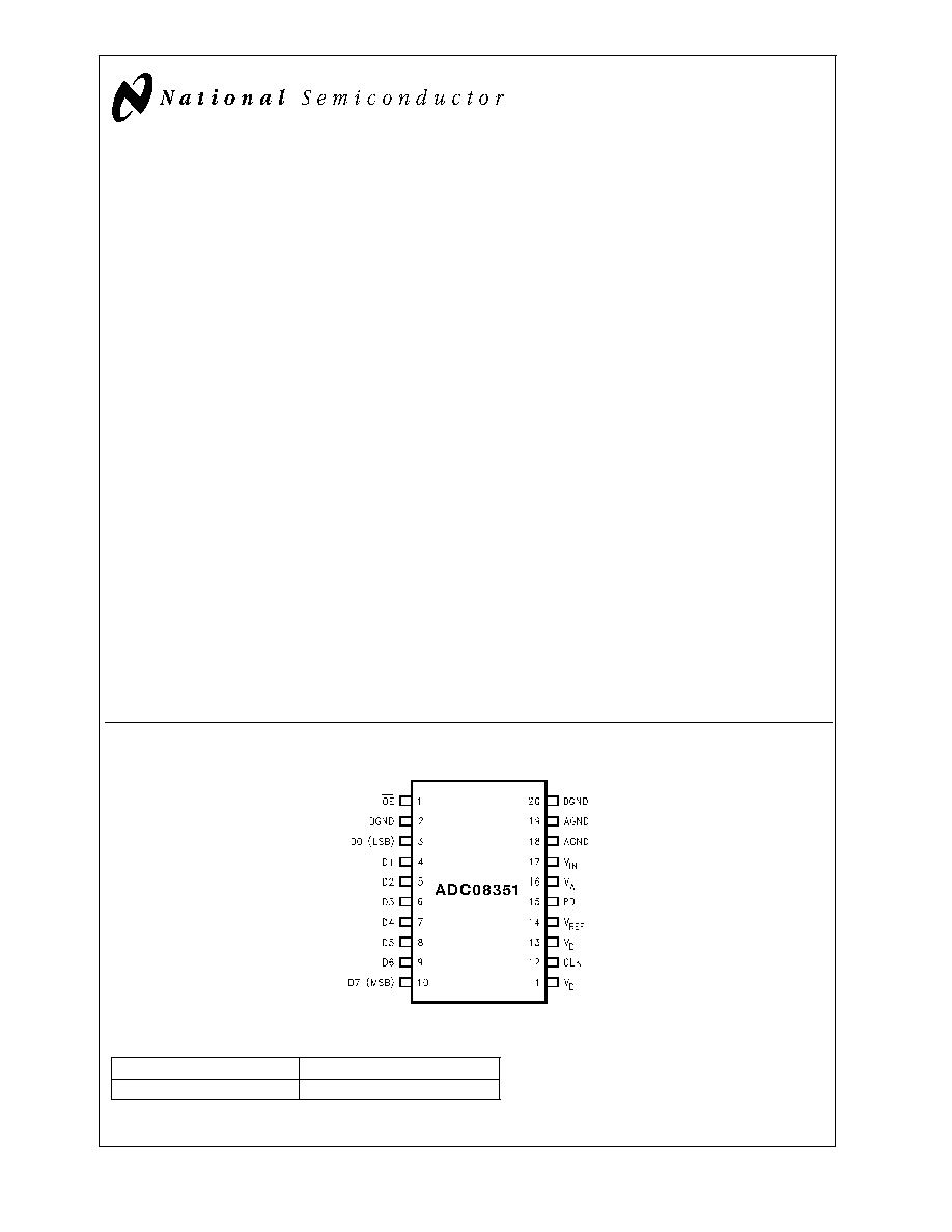
Pin Configuration
Ordering Information
ADC08351CIMTC
TSSOP
ADC08351CIMTCX
TSSOP (tape & reel)
TRI-STATE
Æ
is a registered trademark of National Semiconductor Corporation.
DS100895-1
March 2000
ADC08351
8-Bit,
42
MSPS,
40
mW
A/D
Converter
© 2000 National Semiconductor Corporation
DS100895
www.national.com

ADC08351 Block Diagram
Pin Descriptions and Equivalent Circuits
Pin
No.
Symbol
Equivalent Circuit
Description
17
V
IN
Analog signal input. Conversion range is 0.5 V
P-P
to
0.68 V
A
.
14
V
REF
Positive reference voltage input. Operating range of
this voltage is 0.75V to V
A
. This pin should be
bypassed with a 10 µF tantalum or aluminum
electrolytic capacitor and a 0.1 µF ceramic chip
capacitor.
1
OE
CMOS/TTL compatible digital input that, when low,
enables the digital outputs of the ADC08351. When
high, the outputs are in a high impedance state.
12
CLK
CMOS/TTL compatible digital clock input. V
IN
is
sampled on the falling edge of CLK input.
15
PD
CMOS/TTL compatible digital input that, when high,
puts the ADC08351 into the power down mode,
where it consumes minimal power. When this pin is
low, the ADC08351 is in the normal operating
mode.
3 thru
10
D0≠D7
Conversion data digital output pins. D0 is the LSB,
D7 is the MSB. Valid data is output just after the
rising edge of the CLK input. These pins are
enabled by bringing the OE pin low.
DS100895-2
ADC08351
www.national.com
2

Pin Descriptions and Equivalent Circuits
(Continued)
Pin
No.
Symbol
Equivalent Circuit
Description
11, 13
V
D
Positive digital supply pin. Connect to a clean, quiet
voltage source of +3V. V
A
and V
D
should have a
common supply and be separately bypassed with a
10 µF tantalum or aluminum electrolytic capacitor
and a 0.1 µF ceramic chip capacitor. See Section
3.0 for more information.
2, 20
DGND
The ground return for the digital supply. AGND and
DGND should be connected together close to the
ADC08351.
16
V
A
Positive analog supply pin. Connected to a clean,
quiet voltage source of +3V. V
A
and V
D
should have
a common supply and be separately bypassed with
a 10 µF tantalum or aluminum electrolytic capacitor
and a 0.1 µF ceramic chip capacitor. See Section
3.0 for more information.
18, 19
AGND
The ground return for the analog supply. AGND and
DGND should be connected together close to the
ADC08351 package.
ADC08351
www.national.com
3

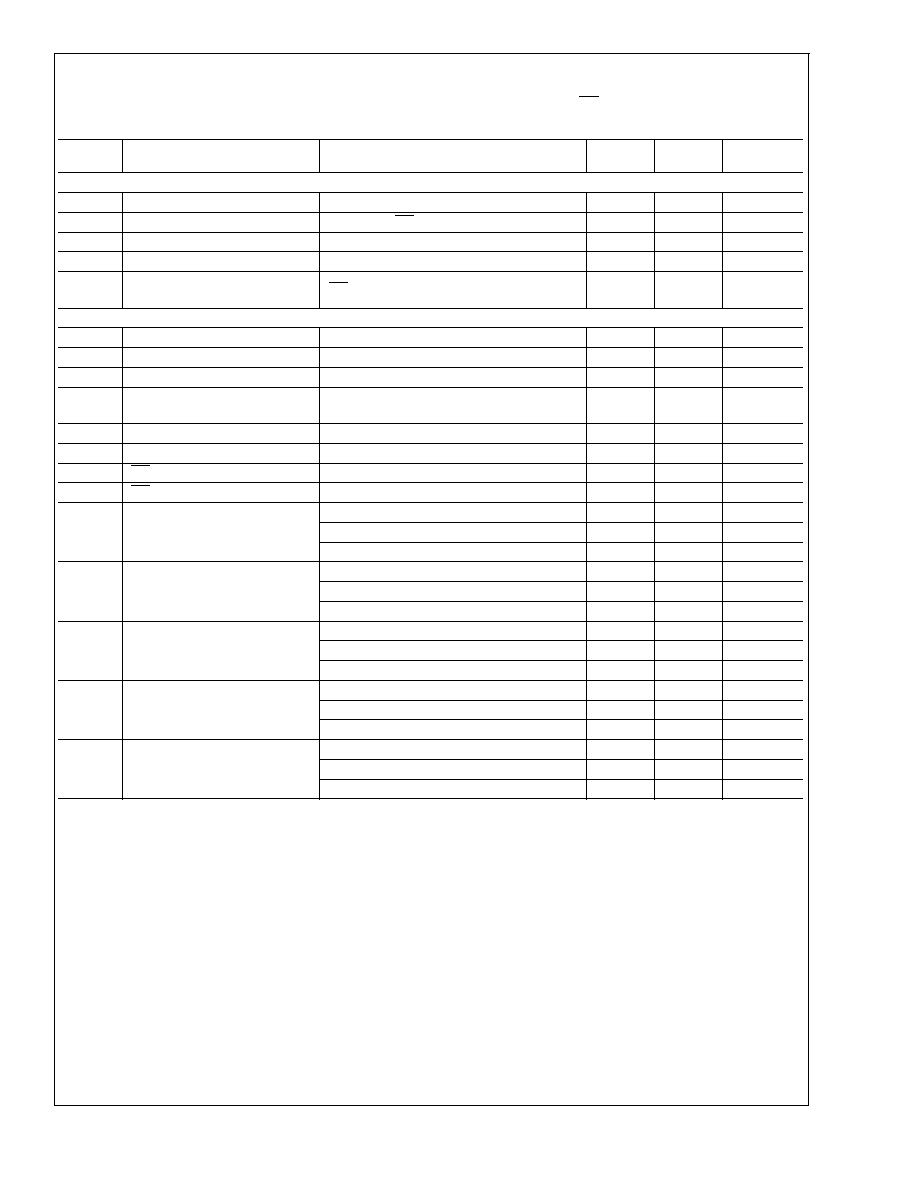
Absolute Maximum Ratings
(Notes 1, 2)
If Military/Aerospace specified devices are required,
please contact the National Semiconductor Sales Office/
Distributors for availability and specifications.
Supply Voltage (V
A
, V
D
)
4.2V
Voltage on Any Input or
Output Pin
-0.3V to 4.2V
Ground Difference
(AGND≠DGND)
±
100 mV
CLK, OE Voltage Range
-0.5 to (V
A
+ 0.5V)
Digital Output Voltage (V
OH
, V
OL
)
V
D
to DGND
Input Current at Any Pin (Note 3)
±
25 mA
Package Input Current (Note 3)
±
50 mA
Package Dissipation at T
A
= 25∞C
(Note 4)
ESD Susceptibility (Note 5)
Human Body Model
4000V
Machine Model
200V
Soldering Temp., Infrared, 10 sec. (Note 6)
300∞C
Storage Temperature
-65∞C to +150∞C
Operating Ratings
(Notes 1, 2)
Operating Temperature Range
-20∞C T
A
+85∞C
Supply Voltage (V
A
, V
D
)
+2.7V to +3.6V
Ground Difference
|DGND≠AGND|
0V to 100 mV
V
IN
Voltage Range (V
P-P
)
0.5V to 0.68 V
A
Converter Electrical Characteristics
The following specifications apply for V
A
= V
D
= +3.0 V
DC
, V
REF
= 2.4V, V
IN
= 1.63 V
P-P
, OE = 0V, C
L
= 20 pF,
f
CLK
= 42 MHz, 50% duty cycle, unless otherwise specified.
Boldface limits apply for T
A
= T
MIN
to T
MAX
: all other limits T
A
= 25∞C (Notes 7, 8)
Symbol
Parameter
Conditions
Typical
(Note 9)
Limits
(Note 9)
Units
(Limits)
DC Accuracy
INL
Integral Non Linearity Error
±
0.7
±
1.4
LSB (max)
DNL
Differential Non Linearity
±
0.6
+1.3
LSB (max)
-1.0
LSB (min)
Missing Codes
0
(max)
E
Z
Zero Scale Offset Error
-17
mV
E
FS
Full Scale Offset Error
-7
mV
Video Accuracy
DP
Differential Phase Error
f
CLK
= 20 MHz, Video Ramp Input
1.0
Degree
DG
Differential Gain Error
f
CLK
= 20 MHz, Video Ramp Input
1.5
%
Analog Input and Reference Characteristics
C
IN
V
IN
Input Capacitance
V
IN
= 1.5V + 0.7 Vrms
(CLK LOW)
4
pF
(CLK HIGH)
11
pF
R
IN
R
IN
Input Resistance
7.2
k
FPBW
Full-Power Bandwidth
120
MHz
V
REF
Reference Input Voltage
At pin 14
0.735
V
V
A
V
I
REF
Reference Input Current
7.7
mA
Power Supply Characteristics
I
A
Analog Supply Current
PD = Low
10.5
mA
PD = High
1
mA
I
D
Digital Supply Current
PD = Low, No Digital Output Load
2.9
mA
PD = High
0.5
mA
Total Operating Current
Excluding Reference Current, V
IN
= 0 V
DC
13.4
16
mA (max)
Power Consumption (active)
PD = Low (excluding reference current)
40.2
48
mW (max)
Power Consumption (power
down)
PD = High (excluding reference current)
<
7
mW
CLK, OE Digital Input Characteristics
V
IH
Logical High Input Voltage
V
D
= V
A
= 3V
2.0
V (min)
V
IL
Logical Low Input Voltage
V
D
= V
A
= 3V
1.0
V (max)
I
IH
Logical High Input Current
V
IH
= V
D
= V
A
= 3.3V
10
µA
I
IL
Logic Low Input Current
V
IL
= 0V, V
D
= V
A
= 3.3V
-10
µA
C
IN
Logic Input Capacitance
10
pF
ADC08351
www.national.com
4
Converter Electrical Characteristics
(Continued)
The following specifications apply for V
A
= V
D
= +3.0 V
DC
, V
REF
= 2.4V, V
IN
= 1.63 V
P-P
, OE = 0V, C
L
= 20 pF,
f
CLK
= 42 MHz, 50% duty cycle, unless otherwise specified.
Boldface limits apply for T
A
= T
MIN
to T
MAX
: all other limits T
A
= 25∞C (Notes 7, 8)
Symbol
Parameter
Conditions
Typical
(Note 9)
Limits
(Note 9)
Units
(Limits)
Digital Output Characteristics
I
OH
High Level Output Current
V
D
= 2.7V, V
OH
= V
D
-0.5V
-1.1
mA (min)
I
OL
Low Level Output Current
V
D
= 2.7V, OE = DGND, V
OL
= 0.4V
1.8
mA (min)
V
OH
High Level Output Voltage
V
D
= 2.7V, I
OH
= -360 µA
2.65
V
V
OL
Low Level Output Voltage
V
D
= 2.7V, I
OL
= 1.6 mA
0.2
V
I
OZH
,
I
OZL
TRI-STATE Output Current
OE = V
D
= 3.3V, V
OH
= 3.3V or V
OL
= 0V
±
10
µA
AC Electrical Characteristics
f
C1
Maximum Conversion Rate
42
MHz (min)
f
C2
Minimum Conversion Rate
2
MHz
t
OD
Output Delay
CLK High to Data Valid
14
19
ns (max)
Pipline Delay (Latency)
2.5
Clock
Cycles
t
DS
Sampling (Aperture) Delay
CLK Low to Acquisition of Data
2
ns
t
OH
Output Hold Time
CLK High to Data Invalid
9
ns
t
EN
OE Low to Data Valid
Loaded as in
Figure 2
14
ns
t
DIS
OE High to High Z State
Loaded as in
Figure 2
10
ns
ENOB
Effective Number of Bits
f
CLK
= 30 MHz, f
IN
= 1 MHz
7.2
Bits
f
CLK
= 42 MHz, f
IN
= 4.4 MHz
7.2
Bits
f
CLK
= 42 MHz, f
IN
= 21 MHz
6.8
6.1
Bits (min)
SINAD
Signal-to-Noise & Distortion
f
CLK
= 30 MHz, f
IN
= 1 MHz
45
dB
f
CLK
= 42 MHz, f
IN
= 4.4 MHz
45
dB
f
CLK
= 42 MHz, f
IN
= 21 MHz
43
38.5
dB (min)
SNR
Signal-to-Noise Ratio
f
CLK
= 30 MHz, f
IN
= 1 MHz
44
dB
f
CLK
= 42 MHz, f
IN
= 4.4 MHz
45
dB
f
CLK
= 42 MHz, f
IN
= 21 MHz
44
41
dB (min)
THD
Total Harmonic Distortion
f
CLK
= 30 MHz, f
IN
= 1 MHz
-57
dB
f
CLK
= 42 MHz, f
IN
= 4.4 MHz
-51
dB
f
CLK
= 42 MHz, f
IN
= 21 MHz
-46
-41
dB (min)
SFDR
Spurious Free Dynamic Range
f
CLK
= 30 MHz, f
IN
= 1 MHz
57
dB
f
CLK
= 42 MHz, f
IN
= 4.4 MHz
54
dB
f
CLK
= 42 MHz, f
IN
= 21 MHz
49
41
dB (min)
Note 1: Absolute Maximum Ratings indicate limits beyond which damage to the device may occur. Operating Ratings indicate conditions for which the device is func-
tional, but do not guarantee specific performance limits. For guaranteed specifications and test conditions, see the Electrical Characteristics. The guaranteed speci-
fications apply only for the test conditions listed. Some performance characteristics may degrade when the device is not operated under the listed test conditions.
Note 2: All voltages are measured with respect to GND = AGND = DGND = 0V, unless otherwise specified.
Note 3: When the input voltage at any pin exceeds the power supplies (that is, less than AGND or DGND, or greater than V
A
or V
D
), the current at that pin should
be limited to 25 mA. The 50 mA maximum package input current rating limits the number of pins that can safely exceed the power supplies with an input current of
25 mA to two.
Note 4: The absolute maximum junction temperature (T
J
max) for this device is 150∞C. The maximum allowable power dissipation is dictated by T
J
max, the
junction-to-ambient thermal resistance (
JA
), and the ambient temperature (T
A
), and can be calculated using the formula P
D
MAX = (T
J
max - T
A
)/
JA
. For the 20-pin
TSSOP,
JA
is 135∞C/W, so P
D
MAX = 926 mW at 25∞C and 481 mW at the maximum operating ambient temperature of 85∞C. Note that the power dissipation of this
device under normal operation will typically be about 68 mW (40 mW quiescent power + 23 mW reference ladder power + 5 mW due to 1 TTL loan on each digital
output). The values for maximum power dissipation listed above will be reached only when the ADC08351 is operated in a severe fault condition (e.g., when input
or output pins are driven beyond the power supply voltages, or the power supply polarity is reversed). Obviously, such conditions should always be avoided.
Note 5: Human body model is 100 pF capacitor discharged through a 1.5 k
resistor. Machine model is 220 pF discharged through ZERO Ohms.
Note 6: See AN-450, "Surface Mounting Methods and Their Effect on Product Reliability", or the section entitled "Surface Mount" found in any post 1986 National
Semiconductor Linear Data Book, for other methods of soldering surface mount devices.
Note 7: All inputs are protected as shown below. Input voltage magnitudes up to 500 mV above the supply voltage or 500 mV below GND will not damage this device.
However, errors in the A/D conversion can occur if the input goes above V
A
or below AGND by more than 300 mV. As an example, if V
A
is 3.0 V
DC
, the full-scale
input voltage must be
3.3 V
DC
to ensure accurate conversions.
ADC08351
www.national.com
5