 | –≠–ª–µ–∫—Ç—Ä–æ–Ω–Ω—ã–π –∫–æ–º–ø–æ–Ω–µ–Ω—Ç: ADC10321 | –°–∫–∞—á–∞—Ç—å:  PDF PDF  ZIP ZIP |
ADC10321
10-Bit, 20MSPS, 98mW A/D Converter with Internal
Sample and Hold
General Description
The ADC10321 is a low power, high performance CMOS
analog-to-digital converter that digitizes signals to 10 bits
resolution at sampling rates up to 25Msps while consuming
a typical 98mW from a single 5V supply. Reference force
and sense pins allow the user to connect an external refer-
ence buffer amplifier to ensure optimal accuracy. No missing
codes is guaranteed over the full operating temperature
range. The unique two stage architecture achieves 9.2 Effec-
tive Bits with a 10MHz input signal and a 20MHz clock fre-
quency. Output formatting is straight binary coding.
To ease interfacing to 3V systems, the digital I/O power pins
of the ADC10321 can be tied to a 3V power source, making
the outputs 3V compatible. When not converting, power con-
sumption can be reduced by pulling the PD (Power Down)
pin high, placing the converter into a low power standby
state, where it typically consumes less than 4mW. The
ADC10321's speed, resolution and single supply operation
makes it well suited for a variety of applications in video, im-
aging, communications, multimedia and high speed data ac-
quisition. Low power, single supply operation ideally suit the
ADC10321 for high speed portable applications, and its
speed and resolution are ideal for charge coupled device
(CCD) input systems.
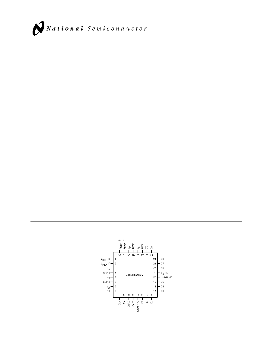
The ADC10321 comes in a space saving 32-pin TQFP and
operates over the industrial (-40∞C
T
A
+85∞C) tempera-
ture range.
Features
n
Internal Sample-and-Hold
n
Single +5V Operation
n
Low Power Standby Mode
n
Guaranteed No Missing Codes
n
Tri-State Outputs
n
TTL/CMOS or 3V Logic Input/Output Compatible
Key Specifications
n
Resolution
10 Bits
n
Conversion Rate
20 Msps
n
ENOB 10MHz Input
9.2 Bits (typ)
n
DNL
0.35 LSB (typ)
n
Conversion Latency
2 Clock Cycles
n
PSRR
56dB
n
Power Consumption
98mW (typ)
n
Low Power Standby Mode
<
4mW (typ)
Applications
n
Digital Video
n
Communications
n
Document Scanners
n
Medical Imaging
n
Electro-Optics
n
Plain Paper Copiers
n
CCD Imaging
Connection Diagram
DS100897-1
January 2000
ADC10321
10-Bit,
20MSPS,
98mW
A/D
Converter
with
Internal
Sample
and
Hold
© 2000 National Semiconductor Corporation
DS100897
www.national.com
Ordering Information
Commercial
(-40∞C
T
A
+85∞C)
NS Package
ADC10321CIVT
TQFP
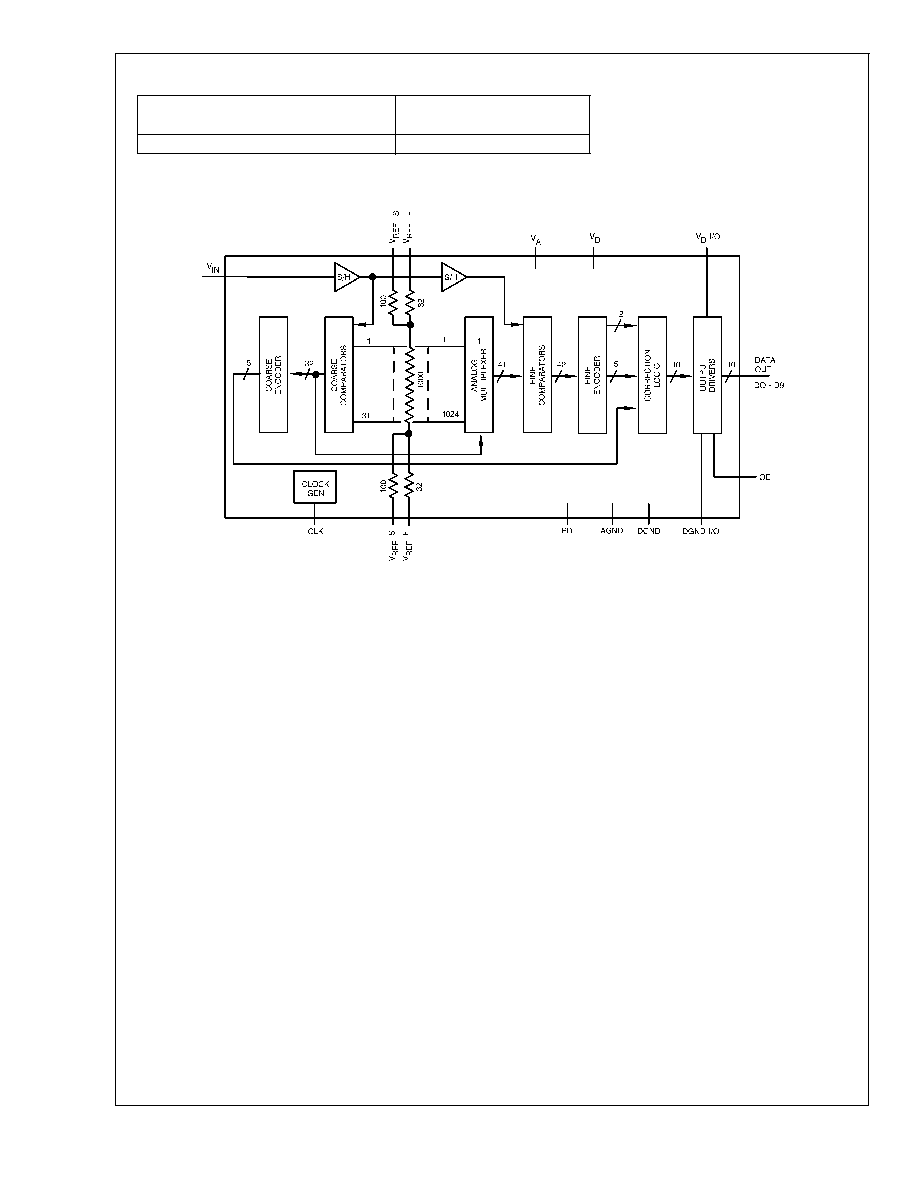
Block Diagram
DS100897-2
ADC10321
www.national.com
2
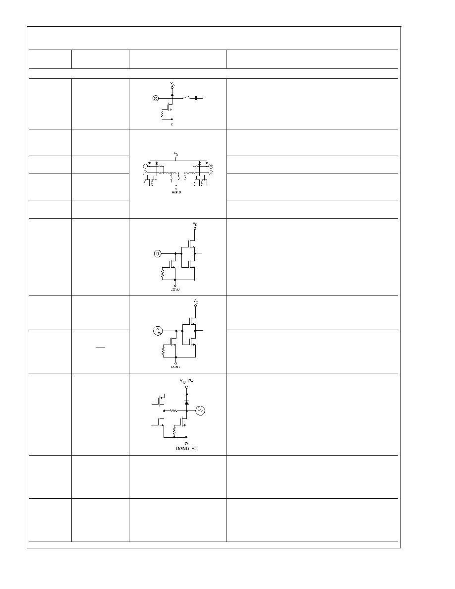
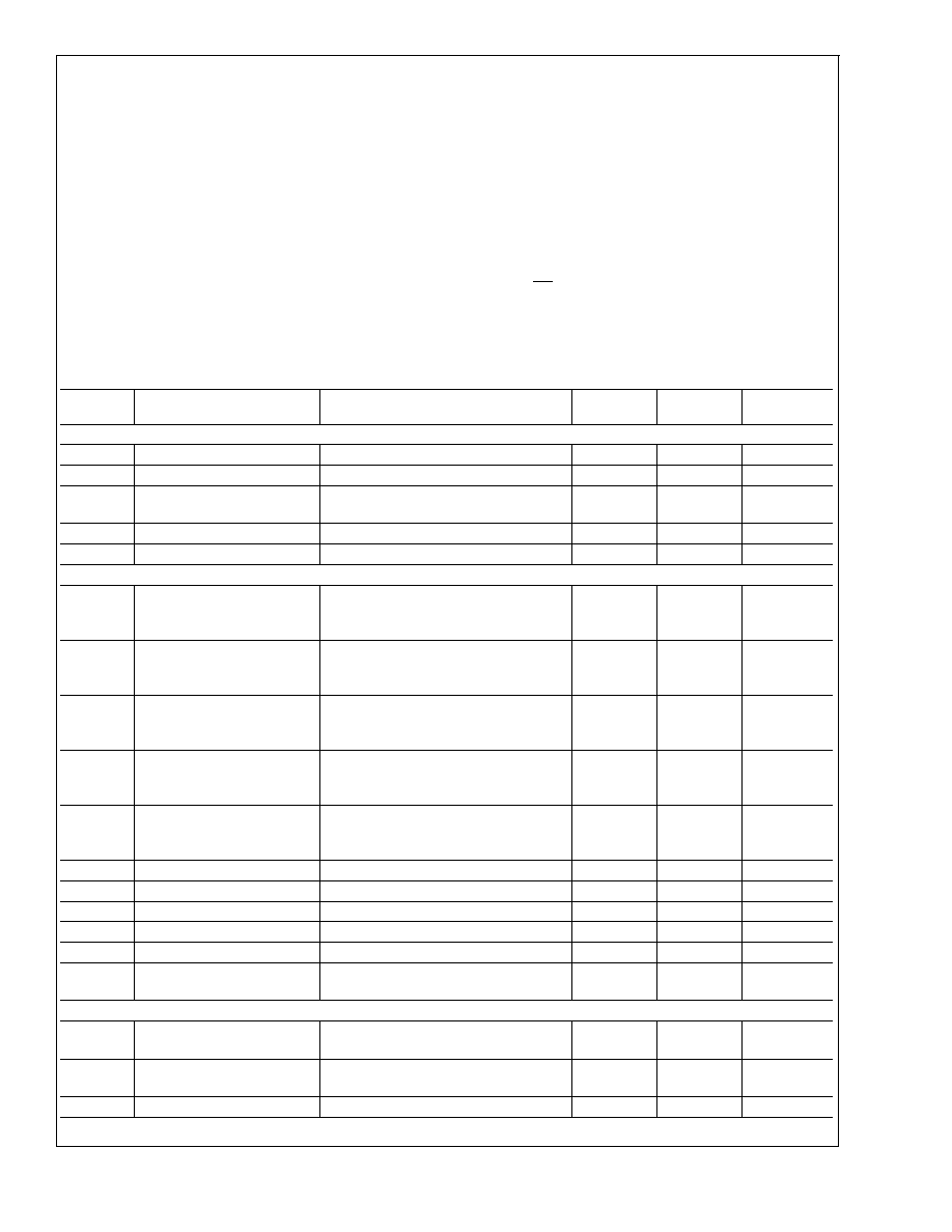
Pin Descriptions and Equivalent Circuits
Pin
No.
Symbol
Equivalent Circuit
Description
Analog I/O
30
V
IN
Analog Input signal to be converted. Conversion
range is V
REF+
S to V
REF-
S.
31
V
REF+
F
Analog input that goes to the high side of the
reference ladder of the ADC. This voltage should
force V
REF+
S to be in the range of 2.3V to 4.0V.
32
V
REF+
S
Analog output used to sense the voltage at the top
of the ADC reference ladder.
2
V
REF-
F
Analog input that goes to the low side of the
reference ladder of the ADC. This voltage should
force V
REF-
S to be in the range of 1.3V to 3.0V.
1
V
REF-
S
Analog output used to sense the voltage at the
bottom of the ADC reference ladder.
9
CLK
Converter digital clock input. V
IN
is sampled on the
falling edge of CLK input.
8
PD
Power Down input. When this pin is high, the
converter is in the Power Down mode and the data
output pins are in a high impedance state.
26
OE
Output Enable pin. When this pin and the PD pin
are low, the output data pins are active. When this
pin or the PD pin is high, the output data pins are in
a high impedance state.
14
thru
19
and
22
thru
25
D0 -D9
Digital Output pins providing the 10 bit conversion
results. D0 is the LSB, D9 is the MSB. Valid data is
present just after the falling edge of the CLK input.
3, 7,
28
V
A
Positive analog supply pins. These pins should be
connected to a clean, quiet voltage source of +5V.
V
A
and V
D
should have a common supply and be
separately bypassed with 10µF to 50µF capacitors
in parallel with 0.1µF capacitors.
5, 10
V
D
Positive digital supply pins. These pins should be
connected to a clean, quiet voltage source of +5V.
V
A
and V
D
should have a common supply and be
separately bypassed with 10µF to 50µF capacitors
in parallel with 0.1µF capacitors.
ADC10321
www.national.com
3
Pin Descriptions and Equivalent Circuits
(Continued)
Pin
No.
Symbol
Equivalent Circuit
Description
Analog I/O
12, 21
V
D
I/O
Positive supply pins for the digital output drivers.
These pins should be connected to a clean, quiet
voltage source of +3V to +5V and be separately
bypassed with 10µF capacitors.
4, 27,
29
AGND
The ground return for the analog supply. AGND and
DGND should be connected together close to the
ADC10321 package.
6, 11
DGND
The ground return for the digital supply. AGND and
DGND should be connected together close to the
ADC10321 pacjage.
13, 20
DGND I/O
The ground return of the digital output drivers.
ADC10321
www.national.com
4
Absolute Maximum Ratings
(Notes 1, 2)
If Military/Aerospace specified devices are required,
please contact the National Semiconductor Sales Office/
Distributors for availability and specifications.
Positive Supply Voltage (V = V
A
= V
D
)
6.5V
Voltage on Any I/O Pin
-0.3V to (V
A
or V
D
) +0.3V)
Input Current at Any Pin (Note 3)
±
25mA
Package Input Current (Note 3)
±
50mA
Package Dissipation at T
A
= 25∞C
See (Note 4)
ESD Susceptibility (Note 5)
Human Body Model
1500V
Machine Model
200V
Soldering Temp., Infrared, 10 sec. (Note 6)
300∞C
Storage Temperature
-65∞C to +150∞C
Operating Ratings
(Notes 1, 2)
Operating Temperature
-40∞C
T
A
+85∞C
V
A,
V
D
Supply Voltage
+4.5V to +5.5V
V
D
I/O Supply Voltage
+2.7V to 5.5V
V
IN
Voltage Range
1.3V to (V
A
-1.0V)
V
REF
+ Voltage Range
2.3V to (V
A
-1.0V)
V
REF
- Voltage Range
1.3V to 3.0V
PD, CLK, OE Voltage
-0.3V to + 5.5V
Converter Electrical Characteristics
The following specifications apply for V
A
= +5.0V
DC
, V
D
= 5.0V
DC
, V
D
I/O = 5.0V
DC
, V
REF
+ = +3.5V
DC
, V
REF
- = +1.5V
DC
,
C
L
= 20pF, f
CLK
= 20MHz, R
S
= 25
. Boldface limits apply for T
A
= T
MIN
to T
MAX
: all other limits T
A
= 25∞C(Note 7)
Symbol
Parameter
Conditions
Typical
(Note 8)
Limits
(Note 9)
Units
Static Converter Characteristics
INL
Integral Non-Linearity
±
0.45
±
1.0
LSB(max)
DNL
Differential-Non Linearity
±
0.35
±
0.85
LSB(max)
Resolution with No Missing
Codes
10
Bits
Zero Scale Offset Error
-6
mV(max)
Full-Scale Error
-6
mV(max)
Dynamic Converter Characteristics
ENOB
Effective Number of Bits
f
IN
= 1.0MHz
f
IN
= 4.43MHz
f
IN
= 10MHz
9.5
9.5
9.2
9.0
Bits
Bits(min)
Bits
S/(N+D)
Signal-to-Noise Plus
Distortion Ratio
f
IN
= 1.0MHz
f
IN
= 4.43MHz
f
IN
= 10MHz
59
59
57
56
dB
dB(min)
dB
SNR
Signal-to-Noise Ratio
f
IN
= 1.0MHz
f
IN
= 4.43MHz
f
IN
= 10MHz
60
60
58
58
dB
dB(min)
dB
THD
Total Harmonic Distortion
f
IN
= 1.0MHz
f
IN
= 4.43MHz
f
IN
= 10MHz
-71
-70
-66
-59
dB
dB(min)
dB
SFDR
Spurious Free Dynamic
Range
f
IN
= 1.0MHz
f
IN
= 4.43MHz
f
IN
= 10MHz
74
72
68
60
dB
dB
dB
DG
Differential Gain Error
f
IN
= 4.43MHz, f
CLK
= 17.72MHz
0.5
%(max)
DP
Differential Phase Error
f
IN
= 4.43MHz, f
CLK
= 17.72MHz
0.5
deg(max)
Overrange Output Code
V
IN
>
V
REF
+
1023
Underrange Output Code
V
IN
<
V
REF
-
0
BW
Full Power Bandwidth
150
MHz
PSRR
Power Supply Rejection
Ratio
Change in Full Scale with 4.5V to
5.5V Supply Change
56
dB
Reference and Analog Input Characteristics
V
IN
Analog Input Range
1.3
4.0
V(min)
V(max)
C
IN
Analog V
IN
Input
Capacitance
5
pF
I
IN
Input Leakage Current
10
µA
ADC10321
www.national.com
5