TL H 11391
ADC10831
ADC10832
ADC10834
ADC10838
10-Bit
Plus
Sign
Serial
IO
AD
Converters
with
MUX
SampleHold
and
Reference
December 1994
ADC10831 ADC10832 ADC10834 ADC10838
10-Bit Plus Sign Serial I O A D Converters
with MUX Sample Hold and Reference
General Description
This series of CMOS 10-bit plus sign successive approxima-
tion A D converters features versatile analog input multi-
plexers sample hold and a 2 5V band-gap reference The
1 2 4 or 8-channel multiplexers can be software configured
for single-ended or differential mode of operation
An input sample hold is implemented by a capacitive refer-
ence ladder and sampled-data comparator This allows the
analog input to vary during the A D conversion cycle
In the differential mode valid outputs are obtained even
when the negative inputs are greater than the positive be-
cause of the 10-bit plus sign output data format
The serial I O is configured to comply with the NSC
MICROWIRE
TM
serial data exchange standard for easy in-
terface to the COPS
TM
and HPC
TM
families of controllers
and can easily interface with standard shift registers and
microprocessors
Applications
Y
Medical instruments
Y
Remote instrumentation
Y
Test equipment
Features
Y
b
5V to
a
5V analog voltage range with
g
5V supplies
Y
Serial I O (MICROWIRE compatible)
Y
1 2 4 or 8-channel differential or single-ended
multiplexer
Y
Software or hardware power down
Y
Analog input sample hold function
Y
Ratiometric or Absolute voltage referencing
Y
No zero or full scale adjustment required
Y
No missing codes over temperature
Y
TTL MOS input output compatible
Y
Standard DIP and SO packages
Key Specifications
Y
Resolution
10 bits plus sign
Y
Dual supply
g
5V
Y
Power dissipation
59 mW (Max)
Y
In power down mode
33 mW
Y
Conversion time
5 ms (Max)
Y
Sampling rate
74 kHz (Max)
Y
Band-gap reference
2 5V
g
2% (Max)
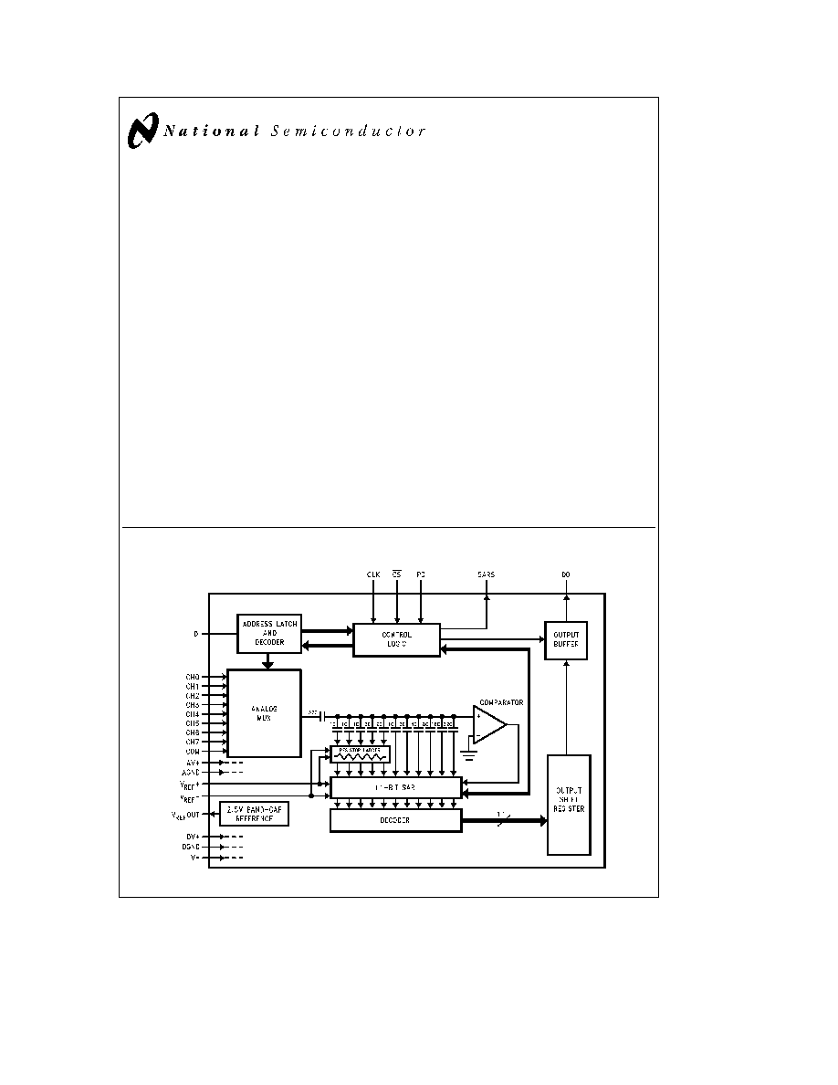
ADC10838 Simplified Block Diagram
TL H 11391 � 1
COPS
TM
HPC
TM
and MICROWIRE
TM
are trademarks of National Semiconductor Corporation
C1995 National Semiconductor Corporation
RRD-B30M75 Printed in U S A
Connection Diagrams for Dual-In-Line and SO Packages
TL H 11391 � 2
Top View
See NS Package Number N16E or M16B
TL H 11391 � 3
Top View
See NS Package Number N20A or M20B
TL H 11391 � 4
Top View
See NS Package Number N20A or M20B
TL H 11391 � 5
Top View
See NS Package Number N24A or M24B
Ordering Information
Industrial Temperature Range
Package
b
40 C
s
T
A
s
a
85 C
ADC10831CIN
N16E
ADC10831CIWM
M16B
ADC10832CIN
N20A
ADC10832CIWM
M20B
ADC10834CIN
N20A
ADC10834CIWM
M20B
ADC10838CIN
N24A
ADC10838CIWM
M24B
2
Absolute Maximum Ratings
(Notes 1
3)
If Military Aerospace specified devices are required
please contact the National Semiconductor Sales
Office Distributors for availability and specifications
Positive Supply Voltage (V
a
e
AV
a
e
DV
a
)
a
6 0V
Negative Supply Voltage (V
b
)
b
6 0V
Total Supply Voltage (V
a
b
V
b
)
12V
Total Reference Voltage (V
REF
a
� V
REF
b
)
a
6 0V
Voltage at Analog Inputs
(CH0-CH7 and COM)
V
a
a
0 3V to V
b
b
0 3V
Voltage at other Inputs and Outputs
V
a
a
0 3V to
b
0 3V
Input Current at Any Pin (Note 4)
30 mA
Package Input Current (Note 4)
120 mA
Package Dissipation at T
A
e
25 C (Note 5)
500 mW
ESD Susceptability (Note 6)
Human Body Model
2500V
Machine Model
150V
Soldering Information
N packages (10 seconds)
260 C
SO Package (Note 7)
Vapor Phase (60 seconds)
215 C
Infrared (15 seconds)
220 C
Storage Temperature
b
40 C to
a
150 C
Operating Ratings
(Notes 2 and 3)
Operating Temperature Range
T
MIN
s
T
A
s
T
MAX
ADC10831CIN ADC10831CIWM
ADC10832CIN ADC10832CIWM
ADC10834CIN ADC10834CIWM
ADC10838CIN ADC10838CIWM
b
40 C
s
T
A
s
a
85 C
Positive Supply Voltage
a
4 5V to
a
5 5V
(V
a
e
AV
a
e
DV
a
)
Negative Supply Voltage (V
b
)
b
4 5V to
b
5 5V
V
REF
a
AV
a
a
50 mV to
b
50 mV
V
REF
b
AV
a
a
50 mV to
b
50 mV
V
REF
(V
REF
a
� V
REF
b
)
a
0 5V to V
a
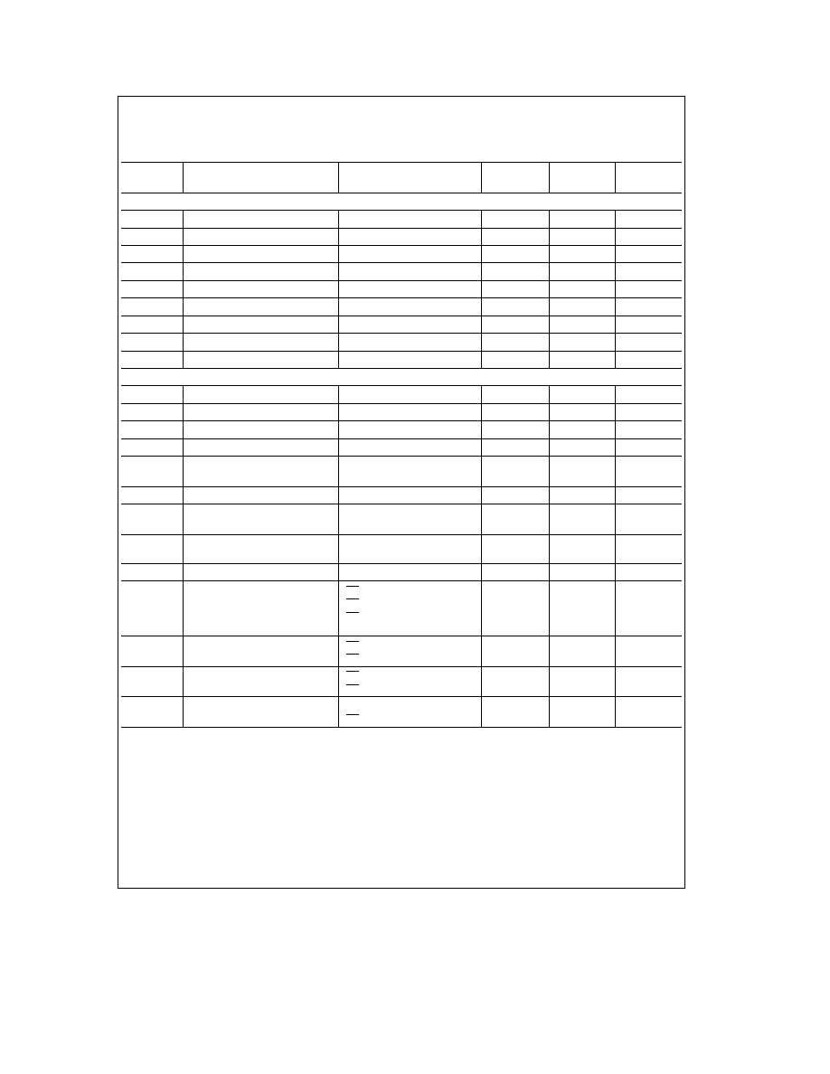
Electrical Characteristics
The following specifications apply for V
a
e
AV
a
e
DV
a
e
a
5 0 V
DC
V
REF
a
e
a
4 096 V
DC
V
REF
b
e
V
IN
b
e
GND
V
b
e b
5 0V
DC
and f
CLK
e
2 5 MHz unless otherwise specified Boldface limits apply for T
A
e
T
J
e
T
MIN
to T
MAX
all
other limits T
A
e
T
J
e a
25 C (Notes 8 9 and 10)
Symbol
Parameter
Conditions
Typical
Limits
Units
(Note 11)
(Note 12)
(Limits)
STATIC CONVERTER CHARACTERISTICS
Resolution with No Missing Codes
10
a
Sign
Bits
TUE
Total Unadjusted Error (Note 13)
g
2 0
LSB(max)
INL
Positive and Negative Integral
g
1 25
LSB(max)
Linearity Error
Positive and Negative
g
1 5
LSB(max)
Full-Scale Error
Offset Error
g
1 5
LSB(max)
Power Supply Sensitivity
Offset Error
V
a
e a
5 0V
g
10%
g
0 2
g
1 0
LSB(max)
a
Full-Scale Error
or V
b
e b
5 0
g
10%
g
0 2
g
1 0
LSB(max)
b
Full-Scale Error
g
0 1
g
0 75
LSB(max)
DC Common Mode Error (Note 14)
V
IN
a
e
V
IN
b
e
V
IN
where
g
0 15
g
0 6
LSB(max)
a
5 0V
t
V
IN
t
b
5V
Multiplexer Channel to
g
0 1
LSB
Channel Matching
3
Electrical Characteristics
(Continued)
The following specifications apply for V
a
e
AV
a
e
DV
a
e
a
5 0 V
DC
V
REF
a
e
a
4 096 V
DC
V
REF
b
e
V
IN
b
e
GND
V
b
e b
5 0 V
DC
and f
CLK
e
2 5 MHz unless otherwise specified Boldface limits apply for T
A
e
T
J
e
T
MIN
to T
MAX
all other limits T
A
e
T
J
e a
25 C (Notes 8 9 and 10) (Continued)
Symbol
Parameter
Conditions
Typical
Limits
Units
(Note 11)
(Note 12)
(Limits)
DYNAMIC CONVERTER CHARACTERISTICS
S (N
a
D)
Signal-to-Noise Plus Distortion Ratio
V
IN
e
8 0 V
PP
Sampling Rate
e
74 kHz
67
dB
and f
IN
e
1 kHz to 15 kHz
ENOB
Effective Number of Bits
V
IN
e
8 0 V
PP
Sampling Rate
e
74 kHz
10 8
Bits
and f
IN
e
1 kHz to 15 kHz
THD
Total Harmonic Distortion
V
IN
e
8 0 V
PP
Sampling Rate
e
74 kHz
b
78
dB
and f
IN
e
1 kHz to 15 kHz
IMD
Intermodulation Distortion
V
IN
e
8 0 V
PP
Sampling Rate
e
74 kHz
b
85
dB
and f
IN
e
1 kHz to 15 kHz
Full-Power Bandwidth
V
IN
e
8 0 V
PP
where
S (N
a
D) Decreases 3 dB
380
kHz
Sampling Rate
e
74 kHz
Multiplexer Channel to Channel Crosstalk
f
IN
e
15 kHz
b
80
dB
Sampling Rate
e
74 kHz
REFERENCE INPUT AND MULTIPLEXER CHARACTERISTICS
Reference Input Resistance
7
kX
5 0
kX(min)
9 5
kX(max)
C
REF
Reference Input Capacitance
70
pF
MUX Input Voltage
V
b
b
50 mV
(min)
AV
a
a
50 mV
(max)
C
IM
MUX Input Capacitance
47
pF
Off Channel Leakage Current (Note 15)
On Channel
e a
5V and
b
0 4
b
3 0
m
A(max)
Off Channel
e b
5V
On Channel
e b
5V and
0 4
3 0
m
A(max)
Off Channel
e a
5V
On Channel Leakage Current (Note 15)
On Channel
e a
5V and
0 4
3 0
m
A(max)
Off Channel
e a
5V
On Channel
e b
5V and
b
0 4
b
3 0
m
A(max)
Off Channel
e a
5V
4
Electrical Characteristics
(Continued)
The following specifications apply for V
a
e
AV
a
e
DV
a
e
a
5 0 V
DC
V
REF
a
e
a
4 096 V
DC
V
REF
b
e
V
IN
b
e
GND
V
b
e b
5 0 V
DC
and f
CLK
e
2 5 MHz unless otherwise specified Boldface limits apply for T
A
e
T
J
e
T
MIN
to T
MAX
all other limits T
A
e
T
J
e a
25 C (Notes 8 9 and 10) (Continued)
Symbol
Parameter
Conditions
Typical
Limits
Units
(Note 11)
(Note 12)
(Limits)
REFERENCE CHARACTERISTICS
V
REF
Out
Reference Output Voltage
2 5V
g
0 5%
2 5V
g
2%
V(max)
D
V
REF
D
T
V
REF
Out Temperature Coefficient
g
40
ppm C
D
V
REF
D
I
L
Load Regulation Sourcing
0 mA
s
I
L
s
a
4 mA
g
0 003
g
0 05
% mA(max)
D
V
REF
D
I
L
Load Regulation Sinking
0 mA
s
I
L
s
b
1 mA
g
0 2
g
0 6
% mA(max)
Line Regulation
5V
g
10%
g
0 3
g
2 5
mV(max)
I
SC
Short Circuit Current
V
REF
Out
e
0V
13
22
mA(max)
Noise Voltage
10 Hz to 10 kHz C
L
e
100 mF
5
m
V
D
V
REF
D
t
Long-term Stability
g
120
ppm kHr
t
SU
Start-Up Time
C
L
e
100 mF
100
ms
DIGITAL AND DC CHARACTERISTICS
V
IN(1)
Logical ``1'' Input Voltage
V
a
e
5 5V
2 0
V(min)
V
IN(0)
Logical ``0'' Input Voltage
V
a
e
4 5V
0 8
V(max)
I
IN(1)
Logical ``1'' Input Current
V
IN
e
5 0V
0 005
a
2 5
m
A(max)
I
IN(0)
Logical ``0'' Input Current
V
IN
e
0V
b
0 005
b
2 5
m
A(min)
V
OUT(1)
Logical ``1'' Output Voltage
V
a
e
4 5V I
OUT
e b
360 mA
2 4
V(min)
V
a
e
4 5V I
OUT
e b
10 mA
4 5
V(min)
V
OUT(0)
Logical ``0'' Output Voltage
V
a
e
4 5V I
OUT
e
1 6 mA
0 4
V(min)
I
OUT
TRI-STATE Output Current
V
OUT
e
0V
b
0 1
b
3 0
m
A(min)
V
OUT
e
5V
a
0 1
a
3 0
m
A(max)
a
I
SC
Output Short-Circuit Source
V
OUT
e
0V V
a
e
4 5V
b
30
b
15
mA(max)
Current
b
I
SC
Output Short-Circuit Sink Current
V
OUT
e
V
a
e
4 5V
30
15
mA(min)
I
D
a
Digital Supply Current
CS
e
HIGH Power Up
0 9
1 3
mA(max)
(Note 17)
CS
e
HIGH Power Down
0 2
0 4
mA(max)
CS
e
HIGH Power Down
0 5
50
m
A(max)
and CLK Off
I
A
a
Positive Analog Supply Current
CS
e
HIGH Power Up
2 7
6 0
mA(max)
(Note 17)
CS
e
HIGH Power Down
3 0
15
m
A(max)
I
A
b
Negative Analog Supply Current
CS
e
HIGH Power Up
b
2 7
b
4 5
mA(min)
(Note 17)
CS
e
HIGH Power Down
b
3 0
b
15
m
A(min)
I
REF
Reference Input Current
V
REF
a
e a
2 5V and
0 6
mA(max)
CS
e
HIGH Power Up
5