ADC10D020
Dual 10-Bit, 20 MSPS, 150 mW A/D Converter
General Description
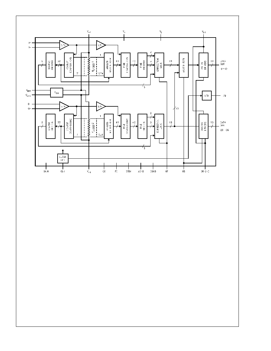
The ADC10D020 is a dual low power, high performance
CMOS analog-to-digital converter that digitizes signals to 10
bits resolution at sampling rates up to 30 MSPS while con-
suming a typical 150 mW from a single 3.0V supply. No
missing codes is guaranteed over the full operating tempera-
ture range. The unique two stage architecture achieves 9.5
Effective Bits over the entire Nyquist band at 20 MHz sample
rate. An output formatting choice of straight binary or 2's
complement coding and a choice of two gain settings eases
the interface to many systems. Also allowing great flexibility
of use is a selectable 10-bit multiplexed or 20-bit parallel
output mode. An offset correction feature minimizes the off-
set error.
To ease interfacing to most low voltage systems, the digital
output power pins of the ADC10D020 can be tied to a
separate supply voltage of 1.5V to 3.6V, making the outputs
compatible with other low voltage systems. When not con-
verting, power consumption can be reduced by pulling the
PD (Power Down) pin high, placing the converter into a low
power state where it typically consumes less than 1 mW and
from which recovery is less than 1 ms. Bringing the STBY
(Standby) pin high places the converter into a standby mode
where power consumption is about 27 mW and from which
recovery is 800 ns.
The ADC10D020's speed, resolution and single supply op-
eration makes it well suited for a variety of applications,
including high speed portable applications.
Operating over the industrial (-40∞
T
A
+85∞C) tempera-
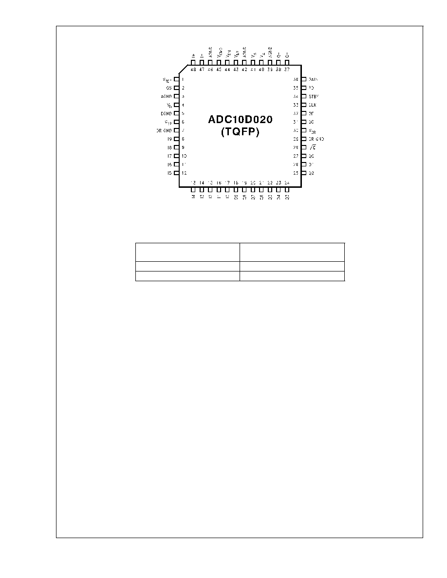
ture range, the ADC10D020 is available in a 48-pin TQFP. An
evaluation board is available to ease the design effort.
Features
n
Internal sample-and-hold
n
Internal reference capability
n
Dual gain settings
n
Offset correction
n
Selectable straight binary or 2's complement output
n
Multiplexed or parallel output bus
n
Single +2.7V to 3.6V operation
n
Power down and standby modes
Key Specifications
n
Resolution
10 Bits
n
Conversion Rate
20 MSPS
n
ENOB
9.5 Bits (typ)
n
DNL
0.35 LSB (typ)
n
Conversion Latency Parallel Outputs
2.5 Clock Cycles
-- Multiplexed Outputs, I Data Bus
2.5 Clock Cycles
-- Multiplexed Outputs, Q Data Bus
3 Clock Cycles
n
PSRR
90 dB
n
Power Consumption -- Normal Operation
150 mW (typ)
-- Power Down Mode
<
1 mW (typ)
-- Fast Recovery Standby Mode
27 mW (typ)
Applications
n
Digital Video
n
CCD Imaging
n
Portable Instrumentation
n
Communications
n
Medical Imaging
n
Ultrasound
April 2002
ADC10D020
Dual
10-Bit,
20
MSPS,
150
mW
A/D
Converter
© 2002 National Semiconductor Corporation
DS200255
www.national.com
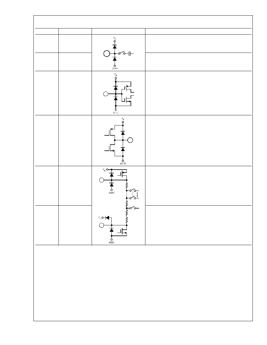
Pin Descriptions and Equivalent Circuits
Pin No.
Symbol
Equivalent Circuit
Description
48
47
I+
I-
Analog inputs to "I" ADC. Nominal conversion range is 1.25V
to 1.75V with GAIN pin low, or 1.0V to 2.0V with GAIN pin
high.
37
38
Q+
Q-
Analog inputs to "Q" ADC. Nominal conversion range is 1.25V
to 1.75V with GAIN pin low, or 1.0V to 2.0V with GAIN pin
high.
1
V
REF
Analog Reference Voltage input. The voltage at this pin
should be in the range of 0.8V to 1.5V. With 1.0V at this pin
and the GAIN pin
low, the full scale differential inputs are
1 V
P-P
. With 1.0V at this pin and the GAIN pin
high, the full
scale differential inputs are 2 V
P-P
. This pin should be
bypassed with a minimum 1 µF capacitor.
45
V
CMO
This is an analog output which can be used as a reference
source and/or to set the common mode voltage of the input. It
should be bypassed with a minimum of 1 µF low ESR
capacitor in parallel with a 0.1 µF capacitor. This pin has a
nominal output voltage of 1.5V and has a 1 mA output source
capability.
43
V
RP
Top of the reference ladder. Do not drive this pin. Bypass
this pin with a 10 µF low ESR capacitor and a 0.1 µF
capacitor.
44
V
RN
Bottom of the reference ladder. Do not drive this pin.
Bypass this pin with a 10 µF low ESR capacitor and a 0.1 µF
capacitor.
ADC10D020
www.national.com
4
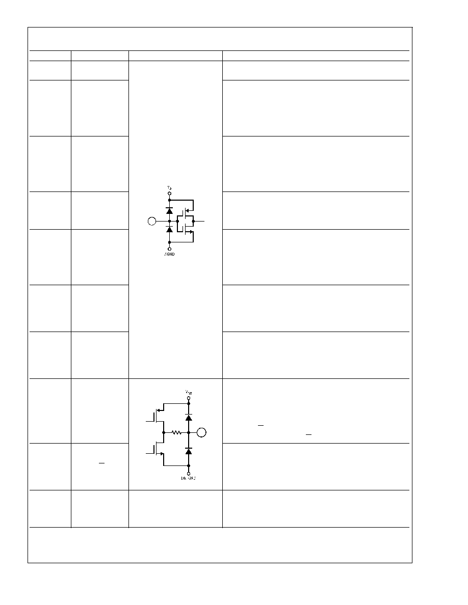
Pin Descriptions and Equivalent Circuits
(Continued)
Pin No.
Symbol
Equivalent Circuit
Description
33
CLK
Digital clock input for both converters. The analog inputs are
sampled on the falling edge of this clock input.
2
OS
Output Bus Select. With this pin at a logic high, both the "I"
and the "Q" data are present on their respective 10-bit output
buses (Parallel mode of operation). When this pin is at a logic
low, the "I" and "Q" data are multiplexed onto the "I" output
bus and the "Q" output lines all remain at a logic low
(multiplexed mode).
31
OC
Offset Correct pin. A low-to-high transition on this pin initiates
an independent offset correction sequence for each converter,
which takes 34 clock cycles to complete. During this time 32
conversions are taken and averaged. The result is subtracted
from subsequent conversions. Each input pair should have 0V
differential value during this entire 34 clock period.
32
OF
Output Format pin. When this pin is LOW the output format is
Straight Binary. When this pin is HIGH the output format is 2's
complement. This pin may be changed asynchronously, but
this will result in errors for one or two conversions.
34
STBY
Standby pin. The device operates normally with a logic low on
this and the PD (Power Down) pin. With this pin at a logic
high and the PD pin at a logic low, the device is in the
standby mode where it consumes just 27 mW of power. It
takes just 800 ns to come out of this mode after the STBY pin
is brought low.
35
PD
Power Down pin that, when high, puts the converter into the
Power Down mode where it consumes less than 1 mW of
power. It takes less than 1 ms to recover from this mode after
the PD pin is brought low. If both the STBY and PD pins are
high simultaneously, the PD pin dominates.
36
GAIN
This pin sets the internal signal gain at the inputs to the
ADCs. With this pin low the full scale differential input
peak-to-peak signal is equal to V
REF
. With this pin high the
full scale differential input peak-to-peak signal is equal to 2 x
V
REF
.
8 thru 27
I0≠I9 and Q0≠Q9
3V TTL/CMOS-compatible Digital Output pins that provide the
conversion results of the I and Q inputs. I0 and Q0 are the
LSBs, I9 and Q9 are the MSBs. Valid data is present just after
the rising edge of the CLK input in the Parallel mode. In the
multiplexed mode, I-channel data is valid on I0 through I9
when the I/Q output is high and the Q-channel data is valid
on I0 through I9 when the I/Q output is low.
28
I/Q
Output data valid signal. In the multiplexed mode, this pin
transitions from low to high when the data bus transitions
from Q-data to I-data, and from high to low when the data bus
transitions from I-data to Q-data. In the Parallel mode, this pin
transitions from low to high as the output data changes.
40, 41
V
A
Positive analog supply pin. This pin should be connected to a
quiet voltage source of +2.7V to +3.6V. V
A
and V
D
should
have a common supply and be separately bypassed with
10 µF to 50 µF capacitors in parallel with 0.1 µF capacitors.
ADC10D020
www.national.com
5