ADC1175
8-Bit, 20MHz, 60mW A/D Converter
General Description
The ADC1175 is a low power, 20 Msps analog-to-digital
converter that digitizes signals to 8 bits while consuming just
60 mW of power (typ). The ADC1175 uses a unique archi-
tecture that achieves 7.5 Effective Bits. Output formatting is
straight binary coding.
The excellent DC and AC characteristics of this device,
together with its low power consumption and +5V single
supply operation, make it ideally suited for many video,
imaging and communications applications, including use in
portable equipment. Furthermore, the ADC1175 is resistant
to latch-up and the outputs are short-circuit proof. The top
and bottom of the ADC1175's reference ladder is available
for connections, enabling a wide range of input possibilities.
The ADC1175 is offered in SOIC (EIAJ) and TSSOP. It is
designed to operate over the commercial temperature range
of -20�C to +75�C.
Features
n
Internal Sample-and-Hold Function
n
Single +5V Operation
n
Internal Reference Bias Resistors
n
Industry Standard Pinout
n
TRI-STATE Outputs
Key Specifications
j
Resolution
8 Bits
j
Maximum Sampling Frequency
20 Msps (min)
j
THD
-55 dB (typ)
j
DNL
0.75 LSB (max)
j
ENOB
7.5 Bits (typ)
j
Guaranteed No Missing Codes
j
Differential Phase
0.5 Degree (typ)
j
Differential Gain
0.4% (typ)
j
Power Consumption
(excluding reference current)
60mW (typ)
Applications
n
Video Digitization
n
Digital Still Cameras
n
Set Top Boxes
n
Communications
n
Medical Imaging
n
Personal Computer Video Cameras
n
Digital Television
n
CCD Imaging
n
Electro-Optics
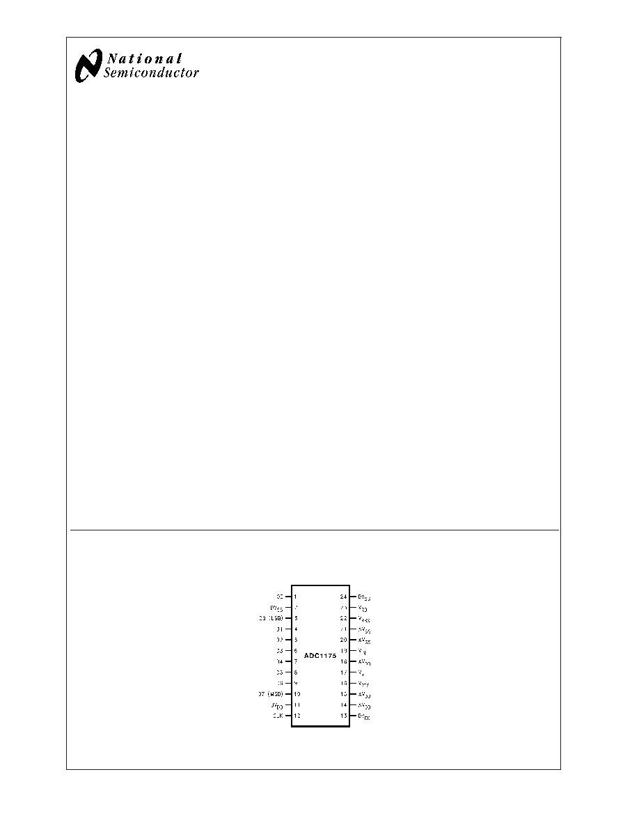
Pin Configuration
ADC1175 Pin Configuration
10009201
March 2003
ADC1
175
8-Bit,
20MHz,
60mW
A/D
Converter
� 2003 National Semiconductor Corporation
DS100092
www.national.com
Ordering Information
ADC1175CIJM
SOIC (EIAJ)
ADC1175CIJMX
SOIC (EIAJ) (tape & reel)
ADC1175CIMTC
TSSOP
ADC1175CIMTCX
TSSOP (tape & reel)
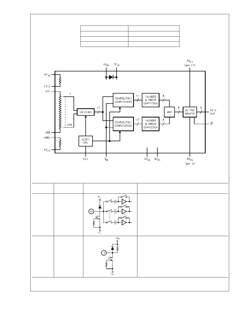
Block Diagram
10009202
Pin Descriptions and Equivalent Circuits
Pin
No.
Symbol
Equivalent Circuit
Description
19
V
IN
Analog signal input. Conversion range is V
RB
to V
RT
.
16
V
RTS
Reference Top Bias with internal pull-up resistor.
Short this pin to V
RT
to self bias the reference ladder.
ADC1
175
www.national.com
2
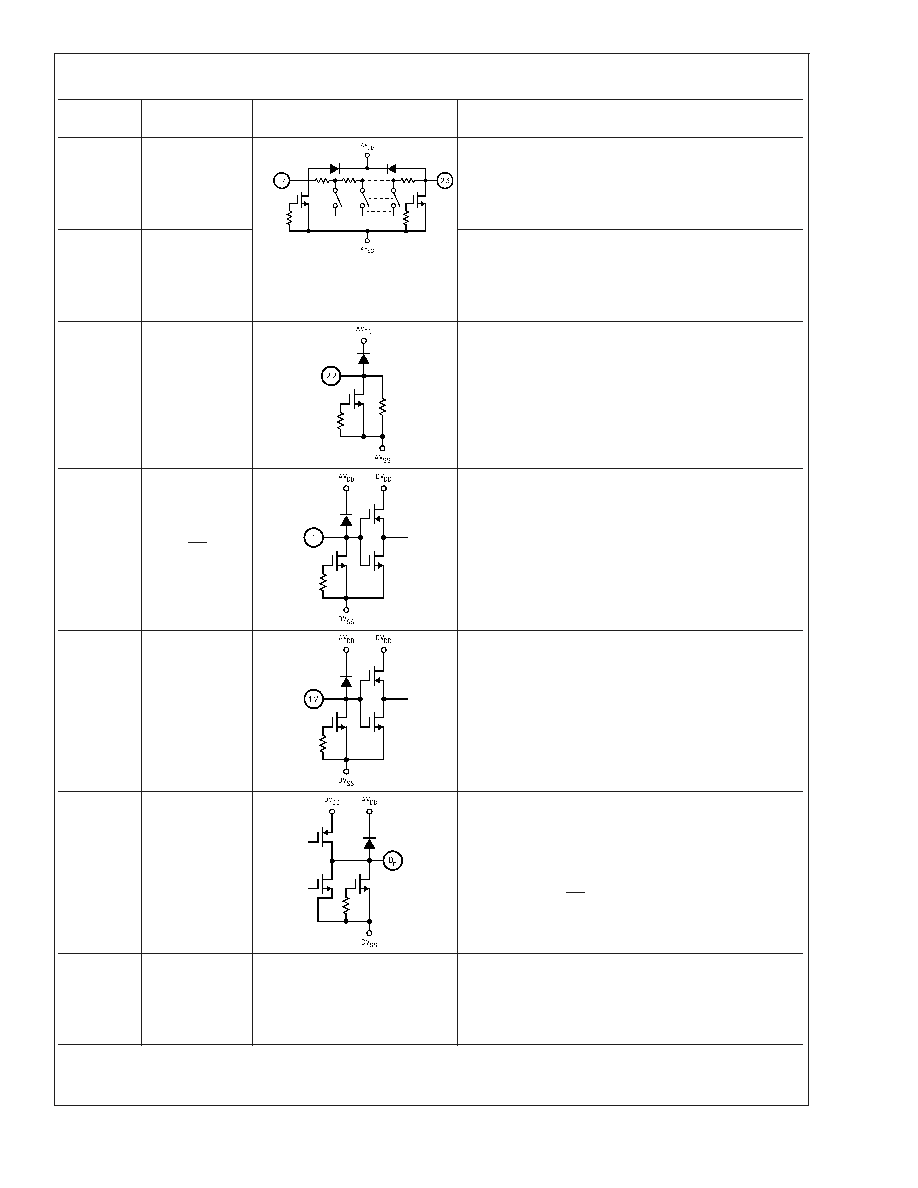
Pin Descriptions and Equivalent Circuits
(Continued)
Pin
No.
Symbol
Equivalent Circuit
Description
17
V
RT
Analog Input that is the high (top) side of the
reference ladder of the ADC. Nominal range is 1.0V
to AV
DD
. Voltage on V
RT
and V
RB
inputs define the
V
IN
conversion range. Bypass well. See Section 2.0
for more information.
23
V
RB
Analog Input that is the low (bottom) side of the
reference ladder of the ADC. Nominal range is 0V to
4.0V. Voltage on V
RT
and V
RB
inputs define the V
IN
conversion range. Bypass well. See Section 2.0 for
more information.
22
V
RBS
Reference Bottom Bias with internal pull down
resistor. Short to V
RB
to self bias the reference
ladder.
1
OE
CMOS/TTL compatible Digital input that, when low,
enables the digital outputs of the ADC1175. When
high, the outputs are in a high impedance state.
12
CLK
CMOS/TTL compatible digital clock Input. V
IN
is
sampled on the falling edge of CLK input.
3 thru
10
D0-D7
Conversion data digital Output pins. D0 is the LSB,
D7 is the MSB. Valid data is output just after the
rising edge of the CLK input. These pins are enabled
by bringing the OE pin low.
11, 13
DV
DD
Positive digital supply pin. Connect to a clean, quiet
voltage source of +5V. AV
DD
and DV
DD
should have
a common source and be separately bypassed with a
10�F capacitor and a 0.1�F ceramic chip capacitor.
See Section 3.0 for more information.
ADC1
175
www.national.com
3

Pin Descriptions and Equivalent Circuits
(Continued)
Pin
No.
Symbol
Equivalent Circuit
Description
2, 24
DV
SS
The ground return for the digital supply. AV
SS
and
DV
SS
should be connected together close to the
ADC1175.
14, 15,
18
AV
DD
Positive analog supply pin. Connected to a clean,
quiet voltage source of +5V. AV
DD
and DV
DD
should
have a common source and be separately bypassed
with a 10 �F capacitor and a 0.1 �F ceramic chip
capacitor. See Section 3.0 for more information.
20, 21
AV
SS
The ground return for the analog supply. AV
SS
and
DV
SS
should be connected together close to the
ADC1175 package.
ADC1
175
www.national.com
4

Absolute Maximum Ratings
(Note 1)
If Military/Aerospace specified devices are required,
please contact the National Semiconductor Sales Office/
Distributors for availability and specifications.
AV
DD
, DV
DD
6.5V
Voltage on Any Pin
-0.3V to 6.5V
V
RT
, V
RB
AV
SS
to AV
DD
CLK, OE Voltage
-0.5 to (AV
DD
+ 0.5V)
Digital Output Voltage
DV
SS
to DV
DD
Input Current (Note 3)
�
25mA
Package Input Current
(Note 3)
�
50mA
Package Dissipation at 25�C
(Note 4)
ESD Susceptibility (Note 5)
Human Body Model
2000V
Machine Model
200V
Soldering Temp., Infrared, 10
sec. (Note 6)
300�C
Storage Temperature
-65�C to +150�C
Operating Ratings
(Notes 1, 2)
Temperature Range
-20�C
T
A
+75�C
AV
DD
, DV
DD
+4.75V to +5.25V
AV
DD
- DV
DD
<
0.5V
|AV
SS
-DV
SS
|
0V to 100 mV
V
RT
1.0V to V
DD
V
RB
0V to 4.0V
V
RT
-V
RB
1V to 2.8V
V
IN
Voltage Range
V
RB
to V
RT
Converter Electrical Characteristics
The following specifications apply for AV
DD
= DV
DD
= +5.0V
DC
, OE = 0V, V
RT
= +2.6V, V
RB
= 0.6V, C
L
= 20 pF,
f
CLK
= 20MHz at 50% duty cycle. Boldface limits apply for T
A
= T
MIN
to T
MAX
; all other limits T
A
= 25�C (Notes 7, 8)
Symbol
Parameter
Conditions
Typical
(Note 9)
Limits
(Note 9)
Units
DC Accuracy
INL
Integral Non Linearity
f
CLK
= 20 MHz
�
0.5
�
1.3
LSB( max)
INL
Integral Non Linearity
f
CLK
= 30 MHz
�
1.0
LSB( max)
DNL
Differential Non Linearity
f
CLK
= 20 MHz
�
0.35
�
0.75
LSB( max)
DNL
Differential Non Linearity
f
CLK
= 30 MHz
�
1.0
LSB( max)
Missing Codes
0
(max)
E
OT
Top Offset
-24
mV
E
OB
Bottom Offset
+37
mV
Video Accuracy
DP
Differential Phase Error
f
in
= 4.43 MHz sine wave,
f
CLK
= 17.7 MHz
0.5
Degree
DG
Differential Gain Error
f
in
= 4.43 MHz sine wave,
f
CLK
= 17.7 MHz
0.4
%
Analog Input and Reference Characteristics
V
IN
Input Range
2.0
V
RB
V
RT
V(min)
V(max)
C
IN
V
IN
Input Capacitance
V
IN
= 1.5V + 0.7Vrms
(CLK LOW)
4
pF
(CLK HIGH)
11
R
IN
R
IN
Input Resistance
>
1
M
BW
Analog Input Bandwidth
120
MHz
R
RT
Top Reference Resistor
360
R
REF
Reference Ladder Resistance
V
RT
to V
RB
300
200
(min)
400
(max)
R
RB
Bottom Reference Resistor
90
I
REF
Reference Ladder Current
V
RT
=V
RTS
, V
RB
=V
RBS
7
4.8
mA (min)
9.3
mA(max)
V
RT
=V
RTS
,V
RB
=AV
SS
8
5.4
mA (min)
10.5
mA(max)
ADC1
175
www.national.com
5