 | –≠–ª–µ–∫—Ç—Ä–æ–Ω–Ω—ã–π –∫–æ–º–ø–æ–Ω–µ–Ω—Ç: CLC109 | –°–∫–∞—á–∞—Ç—å:  PDF PDF  ZIP ZIP |
CLC109
N
CLC109
Low-Power, Wideband, Closed-Loop Buffer
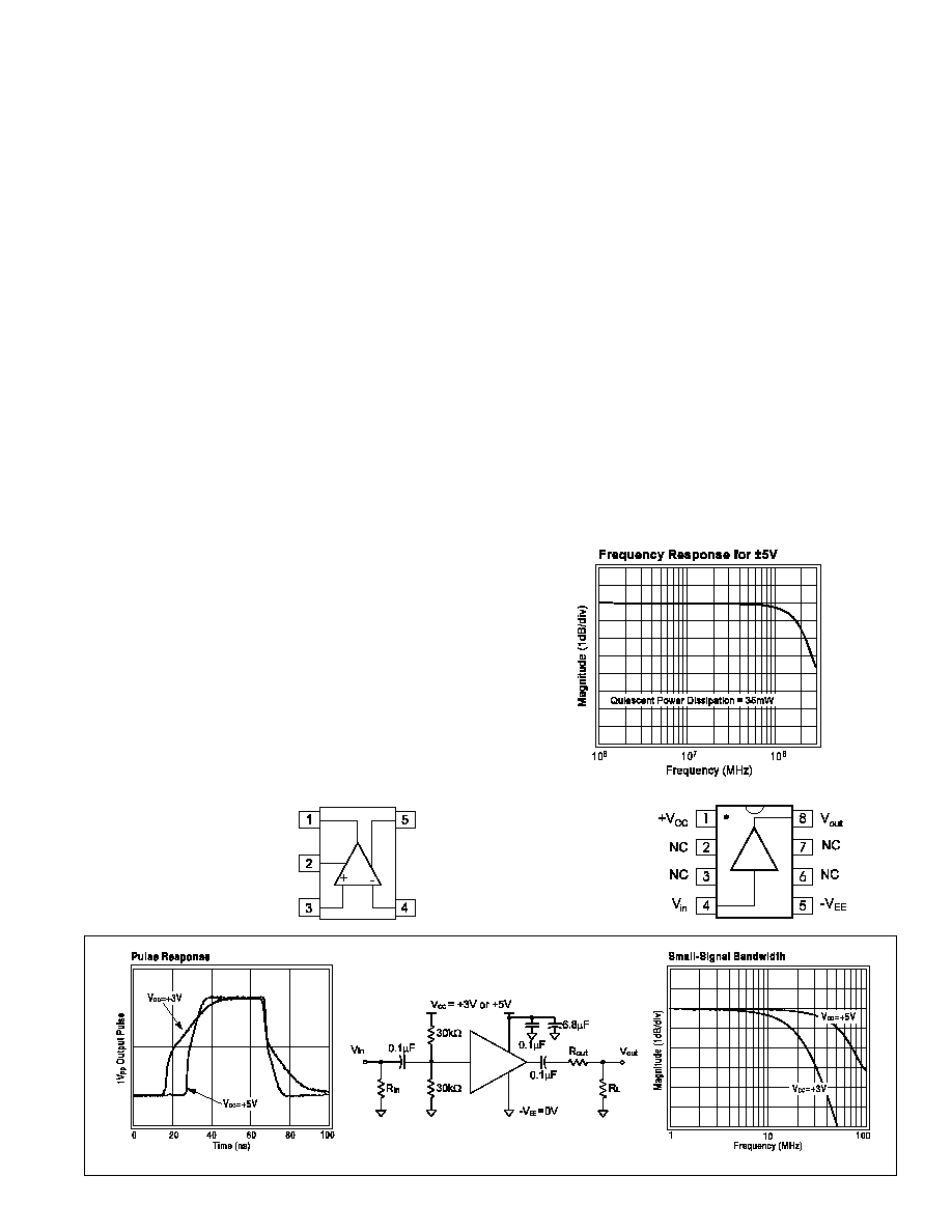
Single-Supply Circuit
Typical Application
General Description
The CLC109 is a high-performance, closed-loop monolithic buffer
intended for power sensitive applications. Requiring only 35mW of
quiescent power (±5V supplies), the CLC109 offers a high bandwidth
of 270MHz (0.5V
pp
) and a slew rate of 350V/
µ
s. Even with this
minimal dissipation, the CLC109 can easily drive a demanding
100
load. The buffer specifications are for a 100
load.
With its patented closed-loop topology, the CLC109 has significant
performance advantages over conventional open-loop designs.
Applications requiring low (2.8
)
output impedance and nearly
ideal unity gain (0.997) through very high frequencies will benefit
from the CLC109's superior performance. Power sensitive
applications will benefit from the CLC109's excellent performance
on reduced or single supply voltages.
Constructed using an advanced, complementary bipolar process
and Comlinear's proven high-performance architectures, the
CLC109 is available in several versions to meet a variety of
requirements.
CLC109AJP
-40∞C to +85∞C
8-pin Plastic DIP
CLC109AJE
-40∞C to +85∞C
8-pin Plastic SOIC
CLC109ALC
-40∞C to +85∞C
dice
CLC109AMC
-55∞C to +125∞C
dice qualified to Method 5008,
MIL-STD-883, Level B
CLC109AJM5
-40∞C to +85∞C
5-pin SOT
Contact factory for other packages and DESC SMD number.
June 1999
CLC109
L
o
w-P
o
w
er
,
Wideband,
Closed-Loop Buff
e
r
PINOUT
DIP & SOIC
Features
s
High small-signal bandwidth (270MHz)
s
Low supply current (3.5mA @ ±5V)
s
Low output impedance (2.8
)
s
350V/
µ
s slew rate
s
Single supply operation (0 to 3V supply min.)
s
Evaluation boards and Spice models
Applications
s
Video switch buffers
s
Test point drivers
s
Low power active filters
s
DC clamping buffer
s
High-speed S & H circuits
s
Inverting op amp input buffer
©
1999 National Semiconductor
Corporation
http://www.national.com
Printed in the U.S.A.
V
inv
V
CC
V
EE
V
o
V
non-inv
PINOUT
SOT23-5
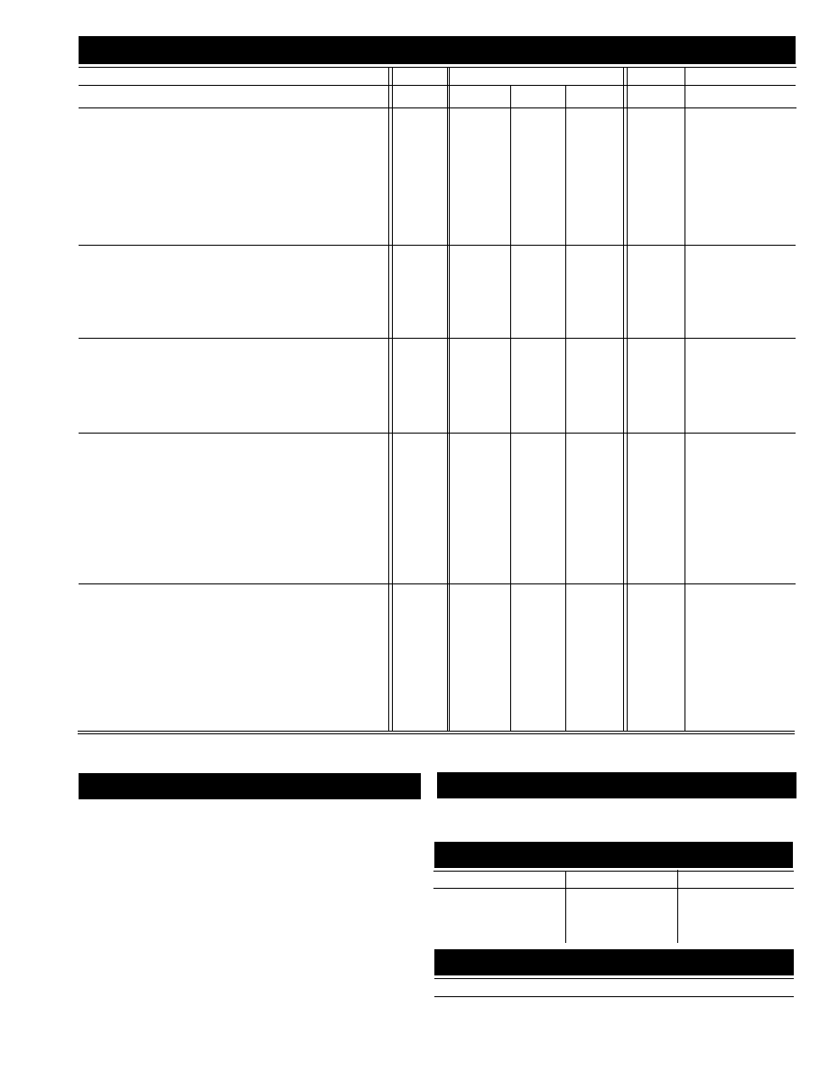
PARAMETER
CONDITIONS
TYP
MIN/MAX RATINGS
UNITS
SYMBOL
Ambient Temperature
CLC109AJ
+25∞C
-40∞C
+25∞C
+85∞C
FREQUENCY RESPONSE
small signal bandwidth
V
out
< 0.5V
pp
270
200
200
150
MHz
SSBW
V
out
< 2.0V
pp
120
90
90
70
MHz
LSBW
gain flatness
V
out
< 0.5V
pp
flatness
DC-30MHz
0
±0.1
±0.1
±0.1
dB
GFL
peaking
DC-200MHz
0
1.0
0.3
0.3
dB
GFPH
rolloff
DC-60MHz
0.1
0.4
0.4
0.6
dB
GFRH
differential gain
4.43MHz, 150
load
0.7
1.5
1.0
1.0
%
DG
differential phase
4.43MHz, 150
load
0.03
0.05
0.05
0.1
∞
DP
TIME DOMAIN RESPONSE
rise and fall time
0.5V step
1.3
1.7
1.7
2.3
ns
TRS
2.0V step
4.4
6
6
7
ns
TRL
settling time to ±0.05%
2.0V step
12
25
18
25
ns
TS
overshoot
0.5V step
3
15
10
10
%
OS1
slew rate
4V step
350
220
250
220
V/
µ
sec
SR
DISTORTION AND NOISE PERFORMANCE
2nd harmonic distortion
2V
pp
, 20MHz
-46
-36
-38
-38
dBc
HD2
3rd harmonic distortion
2V
pp
, 20MHz
-55
-50
-50
-45
dBc
HD3
equivalent output noise
voltage
3.3
4.1
4.1
4.5
nV/
Hz
VN
current
1.3
3
2
2
pA/
Hz
ICN
STATIC DC PERFORMANCE
small signal gain
no load
0.997
0.995
0.995
0.994
V/V
GA1
100
load
0.96
0.94
0.95
0.95
V/V
GA2
output resistance
DC
2.8
5.0
4.0
4.0
RO
*output offset voltage
1
±8.2
±5
±6
mV
VIO
average temperature coefficient
±10
±40
±30
µ
V/∞C
DVIO
* input bias current
±2
±8
±4
±4
µ
A
IBN
average temperature coefficient
±30
±50
±25
nA/∞C
DIBN
power supply rejection ratio
-56
-48
-48
-46
dB
PSRR
* supply current
no load
3.5
4
4
4
mA
ICC
MISCELLANEOUS PERFORMANCE
integral endpoint linearity
±1V, full scale
0.5
1.0
0.7
0.6
%
ILIN
input resistance
1.5
0.3
1.0
2.0
M
RIN
input capacitance
CERDIP
2.5
3.5
3.5
3.5
pF
CIN
Plastic DIP
1.25
2.0
2.0
2.0
pF
CIN
output voltage range
no load
4.0
3.6
3.8
3.8
V
VO
R
L
=100
+3.8,-2.5 +3.0,-1.2 +3.6,-2.0
+3.6,-2.5
V
VOL
R
L
=100
, 0∞C
+3.0,-1.6
V
VOL
output current
+60,-30
+40,-12 +40,-20
+40,-30
mA
IO
0∞C
+40,-16
mA
IO
Min/max ratings are based on product characterization and simulation. Individual parameters are tested as noted. Outgoing quality levels are
determined from tested parameters.
CLC109 Electrical Characteristics
(±V
(±V
(±V
(±V
(±V
cc
cc
cc
cc
cc
= ±5V
= ±5V
= ±5V
= ±5V
= ±5V,,,,, R
R
R
R
R
L
L
L
L
L
= 100
= 100
= 100
= 100
= 100
))
))
)
CLC109 Electrical Characteristics
(±V
CC
= ± 5V, R
L
= 100
unless specified)
Absolute Maximum Ratings
Miscellaneous Ratings
V
cc
±7.0V
I
out
output is short circuit protected to
ground, but maximum reliability will be
maintained if I
out
does not exceed...
30mA
input voltage
±V
cc
maximum junction temperature
+150∞C
operating temperature range
AJ
-40∞C to +85∞C
A8/AM/AL
-55∞C to +125∞C
storage temperature range
-65∞C to +150∞C
lead temperature (soldering 10 sec)
+300∞C
ESD rating
1000V
Notes:
*
AJ : 100% tested at +25∞C.
http://www.national.com
2
Package Thermal Resistance
Package
JC
JA
Plastic (AJP)
70∞C/W
125∞C/W
Surface Mount (AJE)
65∞C/W
145∞C/W
SOT
130∞C/W
200∞C/W
Reliability Information
Transistor count
17
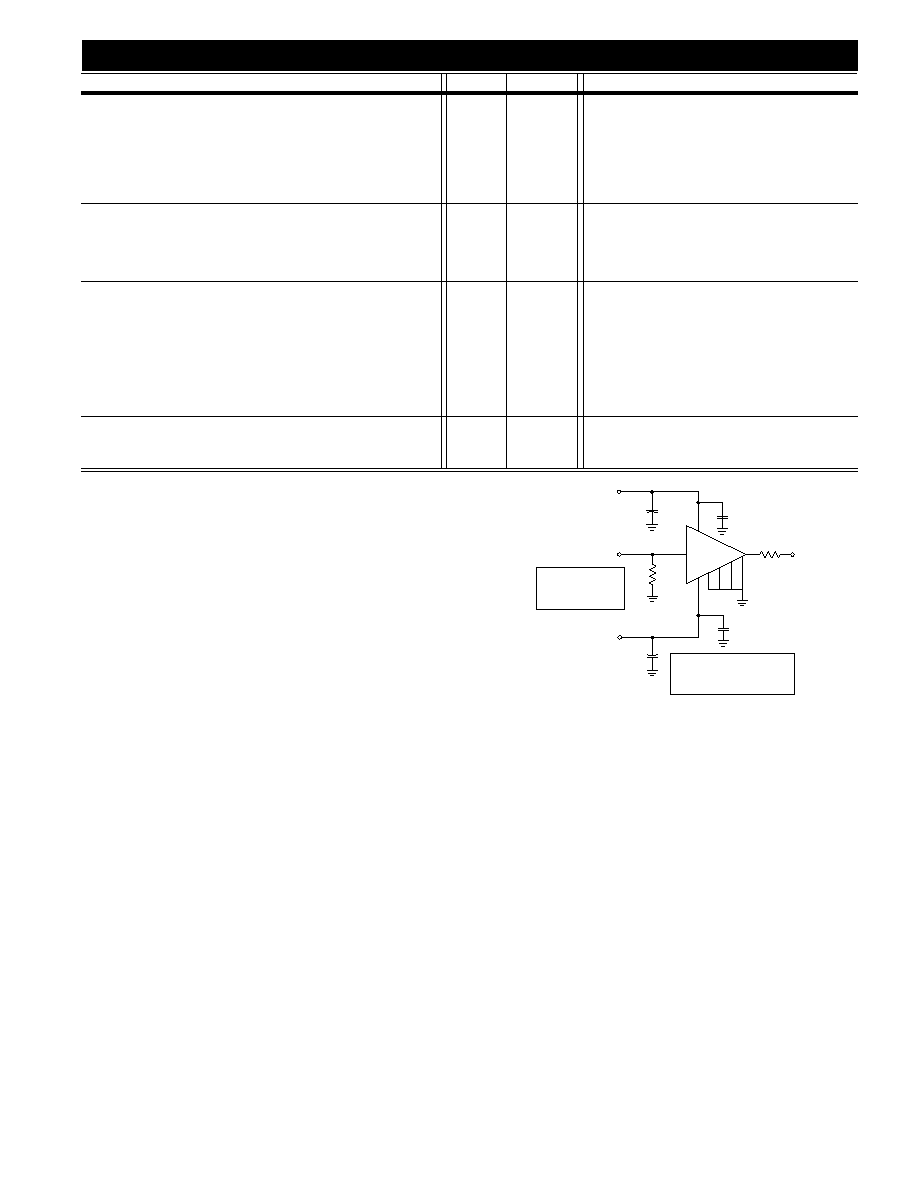
PARAMETERS
CONDITIONS
V
CC
= 3V
V
CC
= 5V
UNITS
FREQUENCY DOMAIN RESPONSE
-3dB bandwidth
V
out
< 0.5V
pp
30
90
MHz
V
out
< 2.0V
pp
35
MHz
gain flatness
V
out
< 0.5V
pp
flatness
DC to 30MHz
3
0.3
dB
peaking
DC to 200MHz
0
0
dB
rolloff
DC to 60MHz
1.5
dB
TIME DOMAIN RESPONSE
rise and fall time
0.5V step
13.9
4.7
ns
2.0V step
13.5
ns
overshoot
0.5V step
0
0
%
slew rate
0.5V step
35
200
V/
µ
s
DISTORTION AND NOISE RESPONSE
2
nd
harmonic distortion
0.5V
pp
,20MHz
-32
dBc
1.0V
pp
,20MHz
-37
dBc
3
rd
harmonic distortion
0.5V
pp
,20MHz
-29
dBc
1.0V
pp
,20MHz
-43
dBc
STATIC DC PERFORMANCE
small-signal gain
AC-coupled
0.89
0.94
V/V
supply current
R
L
=
0.75
1.6
mA
MISCELLANEOUS PERFORMANCE
output voltage range
R
L
=
1.5
2.8
V
pp
R
L
=100
1.1
2.6
V
pp
Electrical Characteristics
(V
CC
=+3V or V
CC
=+5V, -V
ee
= 0V, T
A
=+25∞C, R
L
= 100
, unless noted)
Operation
The CLC109 is a low-power, high-speed unity-gain buffer.
It uses a closed-loop topology which allows for accuracy
not usually found in high-speed buffers. A closed-loop
design provides high accuracy and low output impedance
through a wide bandwidth.
Single Supply Operation
Although the CLC109 is specified to operate from split
±5V power supplies, there is no internal ground reference
that prevents operation from a single voltage power
supply. For single supply operation the input signal should
be biased at a DC value of
Ω
V
CC
. This can be
accomplished by AC coupling and rebiasing as shown in
the "Typical Application" illustrations on the front page.
The above electrical specifications provide typical
performance specifications for the CLC109 at 25∞C while
operating from a single +3V or a single +5V power supply.
Printed Circuit Layout and Supply Bypassing
As with any high-frequency device, a good PCB layout is
required for optimum performance. This is especially
important for a device as fast as the CLC109.
To minimize capacitive feedthrough, pins 2, 3, 6, and 7
should be connected to the ground plane, as shown in
Figure 1. Input and output traces should be laid out as
transmission lines with the appropriate termination resistors
very near the CLC109. On a 0.065 inch epoxy PCB
material, a 50
transmission line (commonly called stripline)
can be constructed by using a trace width of 0.1" over a
complete ground plane.
Figure 1 shows recommended power supply bypassing.
Parasitic or load capacitance directly on the output of the
CLC109 will introduce additional phase shift in the device.
This phase shift can decrease phase margin and increase
frequency response peaking. A small series resistor
inserted between pin 6 and the capacitance effectively
decouples this effect. The graphs on the following page
illustrate the required resistor value and the resulting
performance vs. capacitance.
Precision buffed resistors (PRP8351 series from Precision
Resistive Products), which have low parasitic reactances,
were used to develop the data sheet specifications.
Precision carbon composition resistors or standard spirally-
trimmed RN55D metal film resistors will work, though they
may cause a slight degradation of ac performance due to
their reactive nature at high frequencies.
Evaluation Boards
Evaluation boards are available from National as part
CLC730012 (DIP) and CLC730045 (SOIC). This board
was used in the characterization of the device and provides
optimal performance. Designers are encouraged to copy
these printed circuit board layouts for their applications.
Figure 1: Recommended circuit & evaluation
board schematic
C4
C3
C2
C1
+5V
-5V
0.01
µ
F
0.01
µ
F
6.8
µ
F
6.8
µ
F
+
+
5
4
2
3
6
7
8
1
R
out
V
out
V
in
R
in
CLC109
R
out
is chosen for
desired output impedance.
(CLC109 R
o
= 2.8
)
R
in
is chosen
for desired
input impedance.
3
http://www.national.com

http://www.national.com
4

This page intentionally left blank.
5
http://www.national.com