CLC114
Quad, Low Power Video Buffer
General Description
The CLC114 is a high performance, close loop quad buffer
intended for power sensitive applications. Requiring only
30mW of quiescent power dissipation per channel (
±
5V
supplies), the CLC114 offers a small signal bandwidth of
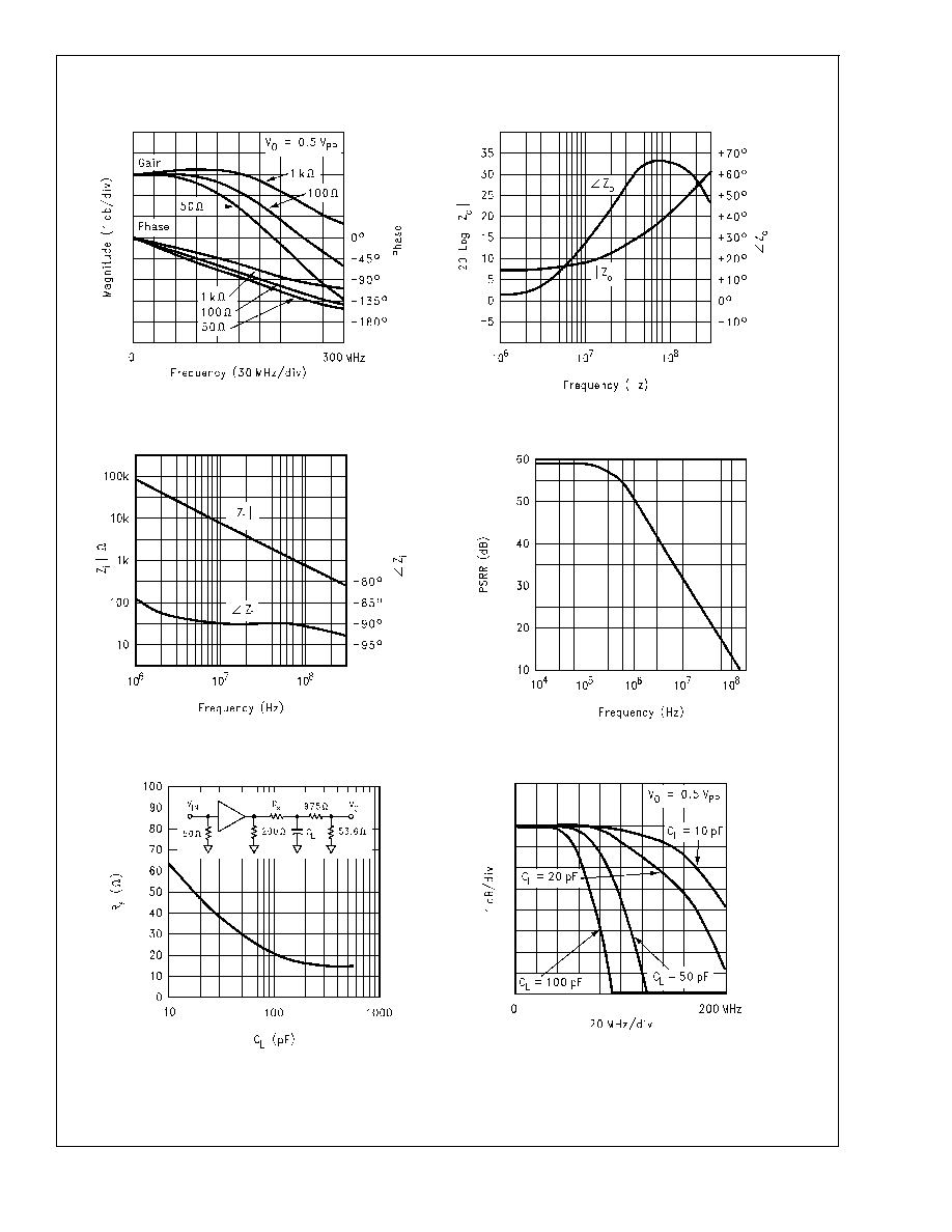
200MHz (0.5Vpp) and a slew rate of 450V/µs.
Designed specifically for high density crosspoint switch and
analog multiplexer applications, the CLC114 offers excellent
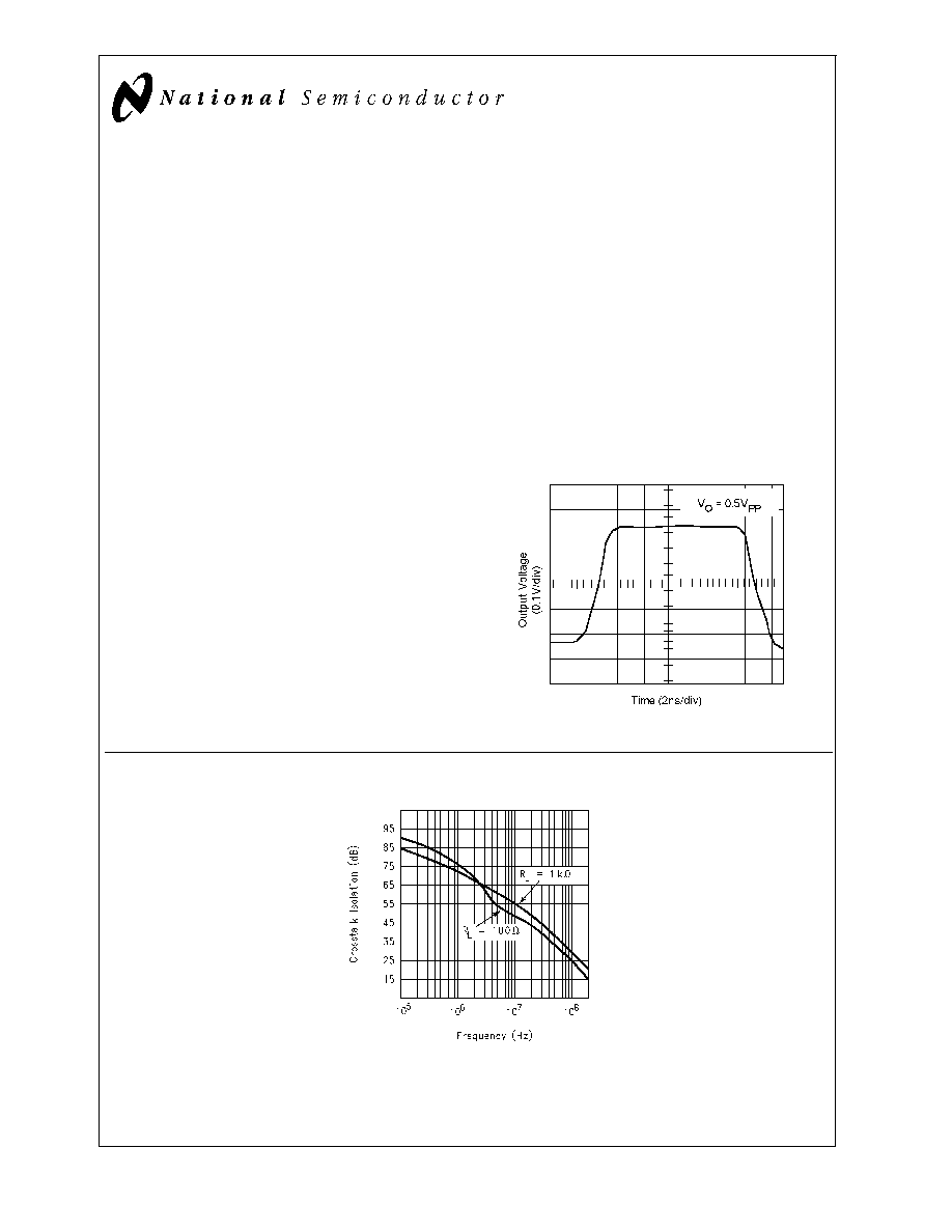
linearity and wide channel isolation (62dB
@
10MHz). Driving
a typical crosspoint switch load, the CLC114 offers differen-
tial gain and phase performance of 0.08% and 0.1% gain
flatness through 30MHz is typically 0.1dB.
With its patented closed loop topology , the CLC114 has
significant performance advantages over conventional open
loop designs. Applications requiring low output impedance
and true unity gain stability through very high frequencies
(active filters, dynamic load buffering, etc.) Will benefit from
the CLC114's superior performance.
Constructed using an advanced, complementary bipolar pro-
cess and National's proven high speed architectures, the
CLC114 is available in several versions to meet a variety of
requirements.
Enhanced Solutions (Military/Aerospace)
SMD Number: 5962-92339
*
Space level versions also available.
*
For more information, visit http://www.national/com/mil
Features
n
Closed loop, quad buffer
n
200MHz small signal bandwidth
n
450V/us slew rate
n
Low power, 30mW per channel (
±
5V sup.)
n
62dB channel isolation (10MHz)
n
Specified for crosspoint switch loads
Applications
n
Video crosspoint switch driver
n
Video distribution buffer
n
Video switching buffer
n
Video signaling multiplexing
n
Instrumentation amps
n
Active filters
Typical Application
Small Signal Pulse Response
DS012738-10
DS012738-21
February 2001
CLC1
14
Quad,
Low
Power
V
ideo
Buffer
© 2001 National Semiconductor Corporation
DS012738
www.national.com

Absolute Maximum Ratings
(Note 1)
If Military/Aerospace specified devices are required,
please contact the National Semiconductor Sales Office/
Distributors for availability and specifications.
Supply Voltage (V
CC
)
±
7V
I
OUT
Output is short circuit protected to
ground, but maximum reliability will
be maintained if I
OUT
does not
exceed...
30mA
Input Voltage
±
V
CC
Maximum Junction Temperature
+150∞C
Operating Temperature Range
-40∞C to +85∞C
Storage Temperature Range
-65∞C to +150∞C
Lead Temperature (Soldering 10 sec)
+300∞C
ESD Rating
500V
Operating Ratings
Thermal Resistance
Package
(
JC
)
(
JA
)
MDIP
65∞C/W
115∞C/W
SOIC
55∞C/W
125∞C/W
Electrical Characteristics
(V
CC
=
±
5 V, R
L
= 100
; Unless Specified)
Symbol
Parameter
Conditions
Typ
Max/Min Ratings
(Note 2)
Units
Ambient Temperature
CLC114AI
+25∞C
-40∞C
+25∞C
+85∞
Frequency Domain Response
SSBW
-3dB Bandwidth
V
OUT
<
0.5V
PP
200
>
135
>
135
>
120
MHz
LSBW
V
OUT
<
2V
PP
95
>
70
>
70
>
70
MHz
Gain Flatness
V
OUT
<
0.5V
PP
GFPL
Peaking
DC to 30MHz
0.0
<
0.3
<
0.2
<
0.3
dB
GFPH
Peaking
30MHz to 200MHz
0.0
<
1.3
<
0.7
<
0.7
dB
GFR
Rolloff
DC to 60MHz
0.1
<
0.8
<
0.8
<
1.0
dB
XT
Crosstalk (All Hostile)
10MHz
62
>
58
>
58
>
60
dB
Time Domain Response
TRS1
Rise and Fall Time
0.5V Step
1.8
<
2.8
<
2.8
<
3.0
ns
TRS2
2V Step
5
<
7
<
7
<
8
ns
TS1
Settling Time to 0.1%
2V Step
10
<
15
<
15
<
20
ns
TS01
to 0.01%
2V Step
20
<
30
<
30
<
40
ns
OS
Overshoot
0.5V Step
3
<
15
<
10
<
15
%
SR
Slew Rate
450
>
180
>
200
>
180
V/µs
Distortion And Noise Response
HD2
2nd Harmonic Distortion
2V
PP
,20MHz
-50
<
-34
<
-38
<
-38
dBc
HD3
3rd Harmonic Distortion
2V
PP
,20MHz
-58
<
-50
<
-50
<
-45
dBc
Equivalent Input Noise
SNF
Noise Floor
>
1MHz
-155
<
-153
<
-153
<
-153
dBm
1Hz
Static, DC Performance
GA
Small Signal Gain
100
Load
0.97
>
0.95
>
0.96
>
0.96
V/V
ILIN
Integral Endpoint Linearity
±
1V, Full Scale
0.4
<
1.0
<
0.6
<
0.5
%
VIO
Output Offset Voltage(Note 3)
±
0.5
<
±
8.2
<
±
5.0
<
±
8.0
mV
DVIO
Average Temperature Coefficient
±
9.0
<
±
40
≠
<
±
30
µV/∞C
IBN
Input Bias Current (Note 3)
±
1.0
<
±
10
<
±
5
<
±
4
µA
DIBN
Average Temperature Coefficient
±
6.0
<
±
62
≠
<
±
25
nA/∞C
PSRR
Power Supply Rejection Ratio
56
>
48
>
48
>
46
dB
ICC
Supply Current, Total (Note 3)
No Load, Quiescent
12.0
<
17.0
<
16.5
<
16.0
mA
Miscellaneous Performance
RIN
Input Resistance
1.5
>
0.3
>
1.0
>
2.0
M
CIN
Input Capacitance
1.8
<
3.5
<
3.0
<
3.5
pF
RO
Output Impedance
DC
2.5
<
5.0
<
3.5
<
3.5
VO
Output Voltage Range
No Load
±
4.0
>
±
3.6
>
±
3.8
>
±
3.8
V
IO
Output Current
25
>
12
>
20
>
25
mA
CLC1
14
www.national.com
3
Electrical Characteristics
(Continued)
(V
CC
=
±
5 V, R
L
= 100
; Unless Specified)
Symbol
Parameter
Conditions
Typ
Max/Min Ratings
(Note 2)
Units
Performance Driving a Crosspoint Switch
Gain Flatness
V
OUT
<
2V
PP
DC to 5MHz
±
0.02
dB
Gain Flatness
V
OUT
<
2V
PP
DC to 30MHZ
±
0.1
dB
Differential Gain
3.58 & 4.43MHz
0.08
%
Differential Phase
3.58 & 4.43MHz
0.1
deg
2nd Harmonic Distortion
5MHz,2V
PP
-60
dBc
30MHz,2V
PP
-43
dBc
3rd Harmonic Distortion
5MHz,2V
PP
-58
dBc
30MHz,2V
PP
-43
dBc
Crosstalk (All Hostile)
5MHz
58
dB
10MHz
54
dB
30MHz
42
dB
Note 1: "Absolute Maximum Ratings" are those values beyond which the safety of the device cannot be guaranteed. They are not meant to imply that the devices
should be operated at these limits. The table of "Electrical Characteristics" specifies conditions of device operation.
Note 2: Min/max ratings are based on product characterization and simulation. Individual parameters are tested as noted. Outgoing quality levels are determined
from tested parameters.
Note 3: AJ-level: spec. is 100% tested at +25∞C.
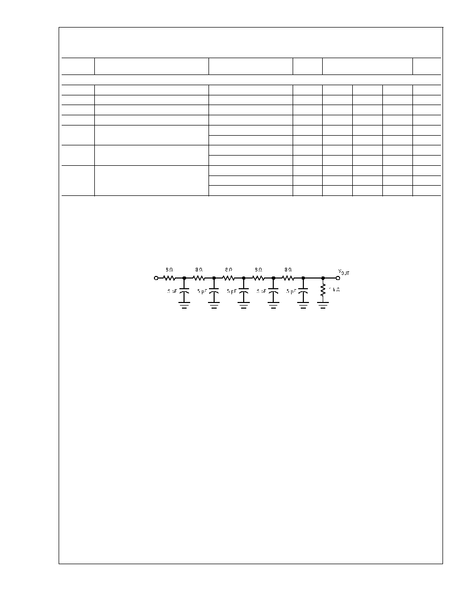
Test Load
DS012738-22
CLC1
14
www.national.com
4