CLC404
Wideband, High Slew Rate, Monolithic Op Amp
General Description
The CLC404 is a high speed, monolithic op amp that com-
bines low power consumption (110mW typical, 120mW
maximum) with superior large signal performance. Operating
off of
±
5V supplies, the CLC404 demonstrates a large signal
bandwidth (5V
PP
output) of 165MHz. The bandwidth perfor-
mance, along with other speed characteristics such as rise
and fall time (2.1ns for a 5V step), is nearly identical to the
small signal performance since slew rate is not limiting factor
in the CLC404 design.
With its 175MHz bandwidth and 10ns settling (0.2%), the
CLC404 is ideal for driving ultra fast flash A/D converters.
The 0.5∞ deviation from linear phase, coupled with -53dBc
2nd harmonic distortion and -60dBc 3rd harmonic distortion
(both at 20MHz), is well suited for many digital and analog
communication applications. These same characteristics,
along with 70mA output current, differential gain of 0.07%,
and differential phase at 0.03∞, make the CLC404 an appro-
priate high performance solution for video distribution and
line driving applications.
Constructed using an advanced, complementary bipolar pro-
cess and proven current feedback topologies, the CLC404
provides performance far beyond that of other monolithic op
amps. The CLC404 is available in several versions to meet a
variety of requirements.
Enhanced Solutions (Military/Aerospace)
SMD Number: 5962-90994
Space level versions also available.
For more information, visit http://www.national.com/mil
Features
n
165MHz large signal bandwidth (5V
PP
)
n
2600V/µs slew rate
n
Low Power: 110mW
n
Low distortion: -53dBc at 20MHz
n
10ns settling to 0.2%
n
0.07% diff. gain, 0.03∞ diff. phase
Applications
n
Fast A/D conversion
n
Line drivers
n
Video distribution
n
High speed communications
n
Radar, IF processors
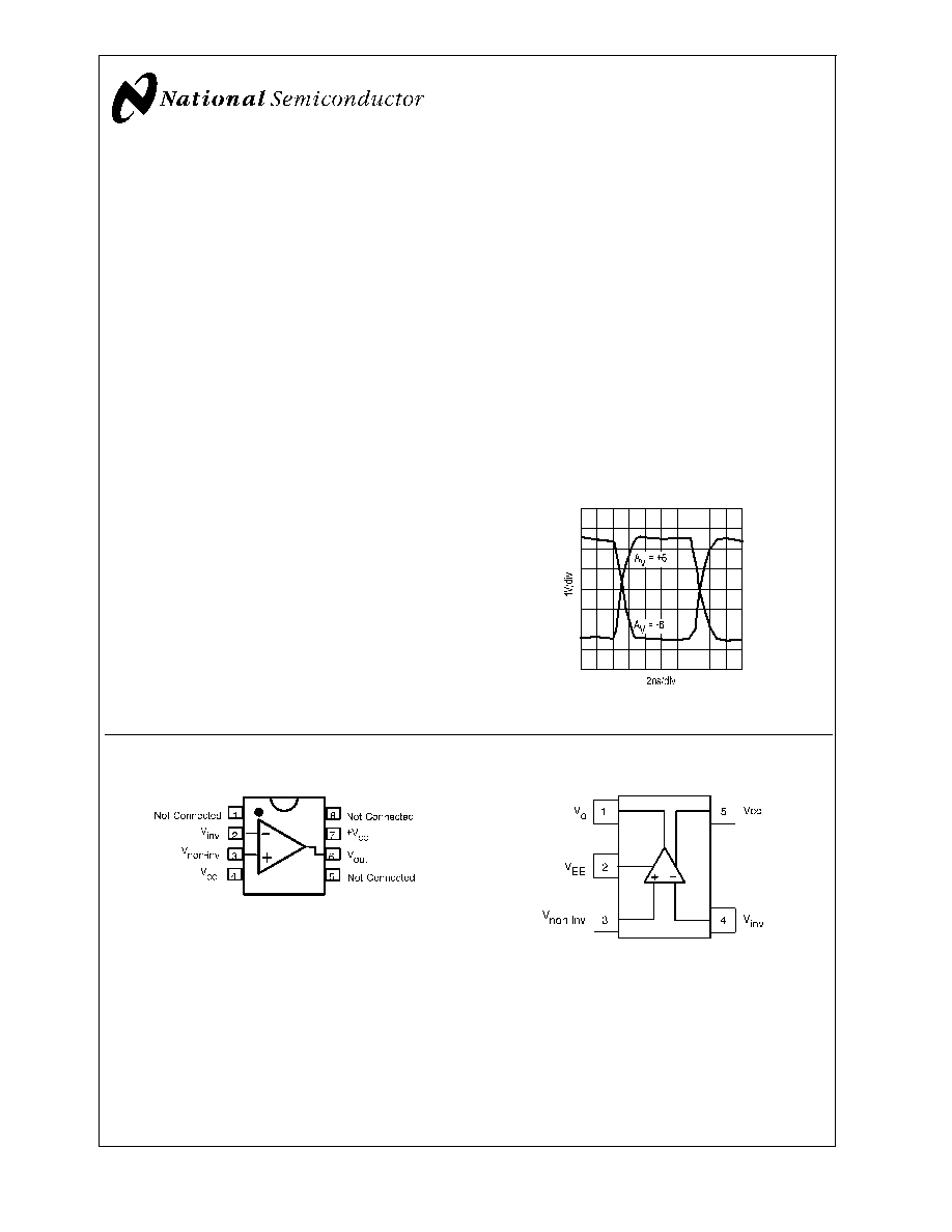
Large Signal Pulse Response
01274607
Connection Diagrams
01274619
Pinout
DIP & SOIC
01274618
Pinout
SOT 23-5
June 2001
CLC404
W
ideband,
High
Slew
Rate,
Monolithic
Op
Amp
© 2001 National Semiconductor Corporation
DS012746
www.national.com

Absolute Maximum Ratings
(Note 1)
If Military/Aerospace specified devices are required,
please contact the National Semiconductor Sales Office/
Distributors for availability and specifications.
Supply Voltage (V
CC
)
±
7V
I
OUT
Output is short circuit protected to
ground, but maximum reliability will
be maintained if I
OUT
does not
exceed...
60mA
Common Mode Input Voltage
±
V
CC
Differential Input Voltage
10V
Junction Temperature
+150∞C
Operating Temperature Range
-40∞C to +85∞C
Storage Temperature Range
-65∞C to +150∞C
Lead Solder Duration (+300∞C)
10 sec
ESD rating (human body model)
500V
Operating Ratings
Thermal Resistance
Package
(
JC
)
(
JA
)
MDIP
65∞C/W
120∞C/W
SOIC
60∞C/W
140∞C/W
Electrical Characteristics
A
V
= +6, V
CC
=
±
5V, R
g
& R
L
=100
, R
f
= 500
; unless specified
Symbol
Parameter
Conditions
Typ
Max/Min Ratings
(Note 2)
Units
Ambient Temperature
CLC404AJ
+25∞C
-40∞C
+25∞C
+85∞C
Frequency Domain Response
SSBW
-3dB Bandwidth
V
OUT
<
2V
PP
175
>
150
>
140
>
120
MHz
LSBW
-3dB Large Signal
V
OUT
<
5V
PP
165
>
140
>
140
>
110
MHz
Gain Flatness
V
OUT
<
2V
PP
GFPL
Peaking
<
40MHz
0
<
0.4
<
0.3
<
0.4
dB
GFPH
Peaking
>
40MHz
0
<
0.7
<
0.5
<
0.7
dB
GFR
Rolloff
<
75MHz
0.2
<
1.0
<
1.1
<
1.3
dB
LPD
Linear Phase Deviation
DC to 75MHz
0.5
<
1.0
<
1.0
<
1.2
deg
Time Domain Response
TRS
Rise and Fall Time
2V Step
2.0
<
2.4
<
2.4
<
2.9
ns
TRL
5V Step
2.1
<
2.6
<
2.6
<
3.2
ns
TS
Settling Time to
±
0.2%
2V Step
10
<
15
<
15
<
15
ns
OS
Overshoot
2V Step
5
<
15
<
12
<
15
%
SR
Slew Rate (Measured at A
V
+2)
(Note 4)
2600
>
2000
>
2000
>
2000
V/µs
Distortion And Noise Response
HD2
2nd Harmonic Distortion
2V
PP
,20MHz
-53
<
-40
<
-45
<
-45
dBc
HD3
3rd Harmonic Distortion
2V
PP
,20MHz
-60
<
-50
<
-50
<
-50
dBc
Equivalent Input Noise
SNF
Noise Floor
>
1MHz
-159
<
-157
<
-157
<
-156
dBm
(1Hz)
INV
Integrated Noise
1MHz to 200MHz
40
<
45
<
45
<
50
µV
DG
Differential Gain (Note 3)
0.07
-
-
-
%
DP
Differential Phase (Note 3)
0.03
-
-
-
∞
Static, DC Performance
VIO
Input Offset Voltage (Note 5)
2
<
±
9.0
<
±
5.0
<
±
10.0
mV
DVIO
Average Temperature Coefficient
30
<
±
50
-
<
±
50
µV/∞C
IBN
Input Bias Current (Note 5)
Non Inverting
15
<
±
44
<
±
22
<
±
22
µA
DIBN
Average Temperature Coefficient
150
<
±
275
-
<
±
200
nA/∞C
IBI
Input Bias Current (Note 5)
Inverting
15
<
±
40
<
±
18
<
±
22
µA
DIBI
Average Temperature Coefficient
150
<
±
275
-
<
±
200
nA/C∞
PSRR
Power Supply Rejection Ratio
52
>
45
>
48
>
45
dB
CMRR
Common Mode Rejection Ration
50
>
44
>
46
>
44
dB
CLC404
www.national.com
2
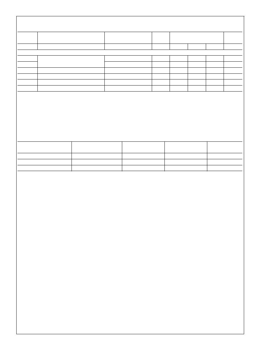
Electrical Characteristics
(Continued)
A
V
= +6, V
CC
=
±
5V, R
g
& R
L
=100
, R
f
= 500
; unless specified
Symbol
Parameter
Conditions
Typ
Max/Min Ratings
(Note 2)
Units
ICC
Supply Current (Note 5)
No Load, Quiescent
11
<
12
<
12
<
12
mA
Miscellaneous Performance
RIN
Non-Inverting Input
Resistance
1000
>
250
>
500
>
1000
k
CIN
Capacitance
1
<
2
<
2
<
2
pF
RO
Output Impedence
At DC
0.1
<
0.3
<
0.2
<
0.2
VO
Output Voltage Range
No Load
±
3.3
>
±
2.8
>
±
3.0
>
±
3.0
V
CMIR
Common Mode Input Range
For Rated Performance
±
2.2
>
±
1.4
>
±
1.8
>
±
2.0
V
IO
Output Current
±
60
>
±
35
>
±
50
>
±
50
mA
Note 1: "Absolute Maximum Ratings" are those values beyond which the safety of the device cannot be guaranteed. They are not meant to imply that the devices
should be operated at these limits. The table of "Electrical Characteristics" specifies conditions of device operation.
Note 2: Max/min ratings are based on product characterization and simulation. Individual parameters are tested as noted. Outgoing quality levels are determined
from tested parameters.
Note 3: Differential gain and phase measured at A
V
+2, R
f
500
,R
L
150
1V
pp
equivalent video signal, 0-100 IRE, 40 IRE
pp
, 0IRE = 0 volts, at 75
load and
3.58MHz. See text.
Note 4: See the text on the back of the datasheet.
Note 5: AJ-level: spec. is 100% tested at +25∞C, sample at 85∞C.
Ordering Information
Package
Temperature Range
Industrial
Part Number
Package Marking
NSC
Drawing
8-pin plastic DIP
-40∞C to +85∞C
CLC404AJP
CLC404AJP
N08E
8-pin plastic SOIC
-40∞C to +85∞C
CLC404AJE
CLC404AJE
M08A
5-pin SOT
-40∞C to +85∞C
CLC404AJM5
A16
MA05A
CLC404
www.national.com
3
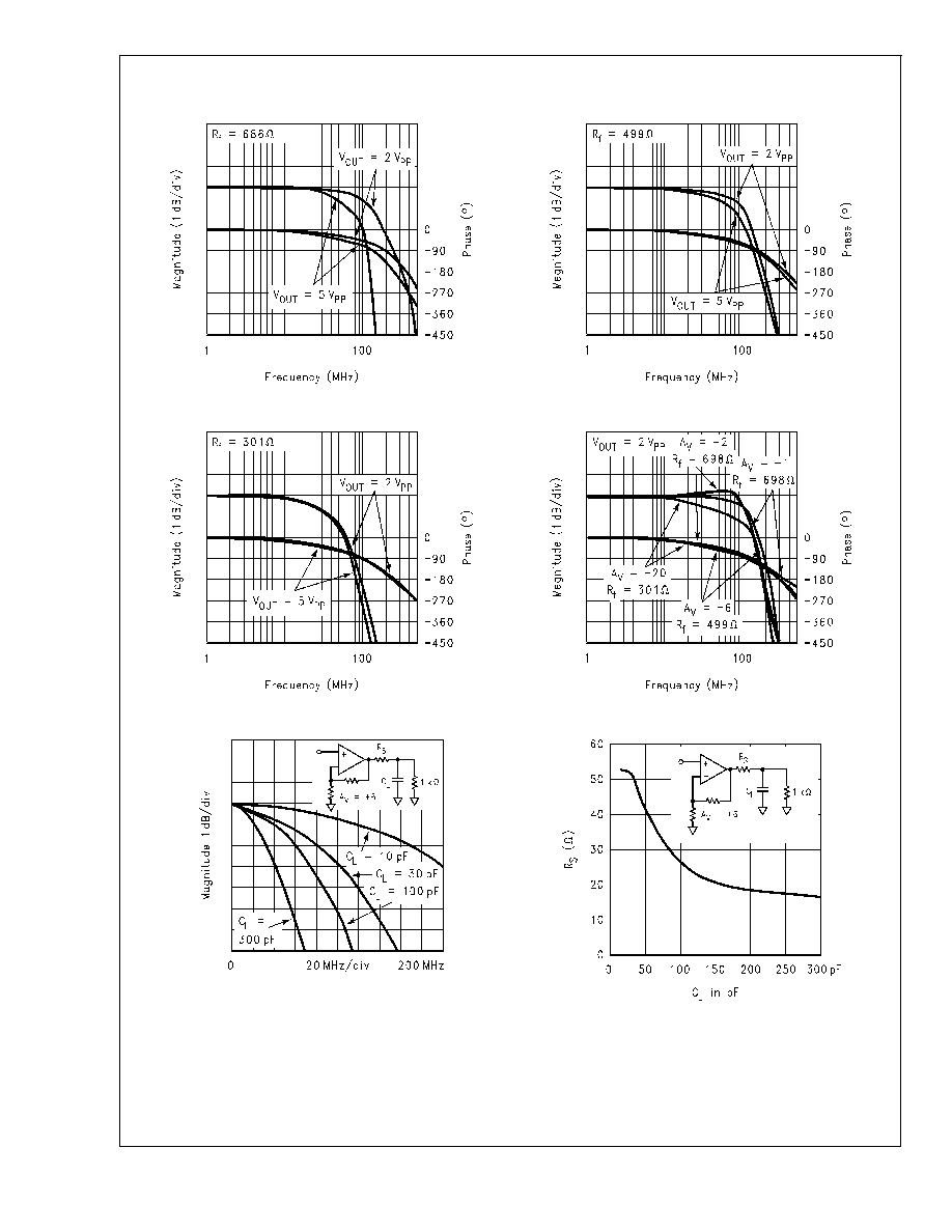
Typical Performance Characteristics
Frequency Response A
V
= +2V/V
Frequency Response A
V
= +6V/V
01274601
01274602
Frequency Response A
V
= +20V/V
Inverting Frequency Response
01274603
01274604
Bandwidth vs Load Capacitance
Recommended R
S
vs Load Capacitance
01274605
01274606
CLC404
www.national.com
4
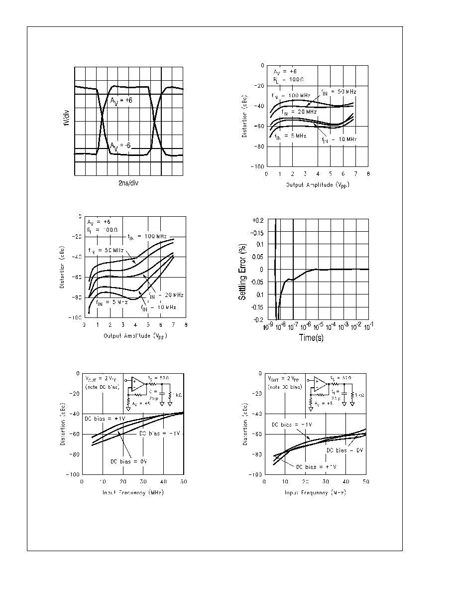
Typical Performance Characteristics
(Continued)
Large Signal Pulse Response
2nd Harmonic Dist. vs. Amplitude
01274607
01274608
3rd Harmonic Dist. vs. Amplitude
Settling Time
01274609
01274610
2nd Harmonic Distortion C
L
= 25pF
3rd Harmonic Distortion C
L
= 25pF
01274611
01274612
CLC404
www.national.com
5