 | –≠–ª–µ–∫—Ç—Ä–æ–Ω–Ω—ã–π –∫–æ–º–ø–æ–Ω–µ–Ω—Ç: CLC405 | –°–∫–∞—á–∞—Ç—å:  PDF PDF  ZIP ZIP |
Frequency Response (A
v
= +2V/V)
Features
s
Low-cost
s
Very low input bias current: 100nA
s
High input impedance: 6M
s
110MHz -3dB bandwidth (A
v
= +2)
s
Low power: I
cc
= 3.5mA
s
Ultra-fast enable/disable times
s
High output current: 60mA
Applications
s
Desktop video systems
s
Multiplexers
s
Video distribution
s
Flash A/D driver
s
High-speed switch/driver
s
High-source impedance applications
s
Peak detector circuits
s
Professional video processing
s
High resolution monitors
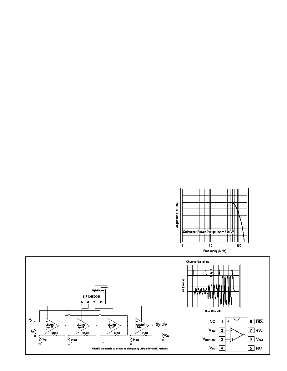
Typical Application
Wideband Digitally Controlled
Programmable Gain Amplifier
Pinout
DIP & SOIC
General Description
The CLC405 is a low-cost, wideband (110MHz) op amp featur-
ing a TTL-compatible disable which quickly switches off in 18ns
and back on in 40ns. While disabled, the CLC405 has a very high
input/output impedance and its total power consumption drops to
a mere 8mW. When enabled, the CLC405 consumes only 35mW
and can source or sink an output current of 60mA.
These
features make the CLC405 a versatile, high-speed solution for
demanding applications that are sensitive to both power and cost.
Utilizing National's proven architectures, this current feedback
amplifier surpasses the performance of alternative solutions and
sets new standards for low power at a low price. This power-
conserving op amp achieves low distortion with -72dBc and
-70dBc for second and third harmonics respectively. Many high
source impedance applications will benefit from the CLC405's
6M
input impedance. And finally, designers will have a bipolar
part with an exceptionally low 100nA non-inverting bias current.
With 0.1dB flatness to 50MHz and low differential gain and phase
errors, the CLC405 is an ideal part for professional video
processing and distribution. However, the 110MHz -3dB band-
width (A
v
= +2) coupled with a 350V/
µ
s slew rate also make the
CLC405 a perfect choice in cost-sensitive applications such as
video monitors, fax machines, copiers, and CATV systems.
CLC405
Low-Cost, Low-Power, 110MHz Op Amp with Disable
N
June 1999
CLC405
Lo
w-Cost,
Lo
w-P
o
wer
,
110MHz Op Amp with Disab
le
© 1999 National Semiconductor Corporation
http://www.national.com
Printed in the U.S.A.
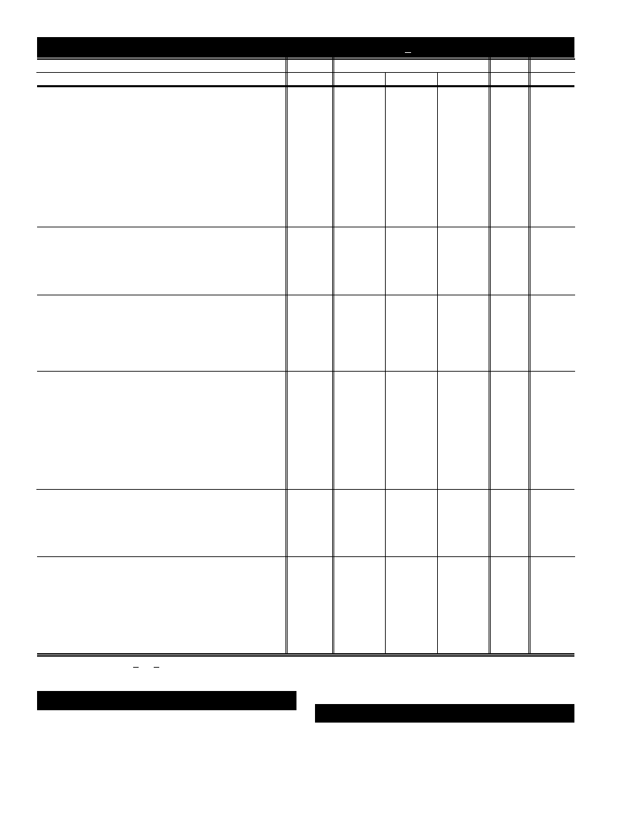
PARAMETERS
CONDITIONS
TYP
MIN/MAX RATINGS
UNITS
NOTES
Ambient Temperature
CLC405AJ
+25∞C
+25∞C
0 to 70∞C
-40 to 85∞C
FREQUENCY DOMAIN RESPONSE
-3dB bandwidth
V
out
< 1.0V
pp
110
75
50
45
MHz
V
out
< 5.0V
pp
42
31
27
26
MHz
1
-3dB bandwidth A
V
= +1
V
out
< 0.5V
pp
(R
f
= 2K)
135
MHz
±0.1dB bandwidth
V
out
< 1.0V
pp
50
15
MHz
gain flatness
V
out
< 1.0V
pp
peaking
DC to 200MHz
0
0.6
0.8
1.0
dB
rolloff
<30MHz
0.05
0.3
0.4
0.5
dB
linear phase deviation
<20MHz
0.3
0.6
0.7
0.7
deg
differential gain
NTSC, R
L
=150
0.01
0.03
0.04
0.05
%
NTSC, R
L
=150
(Note 2)
0.01
%
2
differential phase
NTSC, R
L
=150
0.25
0.4
0.5
0.55
deg
NTSC, R
L
=150
(Note 2)
0.08
deg
2
TIME DOMAIN RESPONSE
rise and fall time
2V step
5
7.5
8.2
8.4
ns
settling time to 0.05%
2V step
18
27
36
39
ns
overshoot
2V step
3
12
12
12
%
slew rate
A
V
= +2
2V step
350
260
225
215
V/
µ
s
A
V
= -1
1V step
650
V/
µ
s
DISTORTION AND NOISE RESPONSE
2
nd
harmonic distortion
2V
pp
, 1MHz/10MHz
-72/-52
-46
-45
-44
dBc
B
3
rd
harmonic distortion
2V
pp
, 1MHz/10MHz
-70/-57
-50
-47
-46
dBc
B
equivalent input noise
non-inverting voltage
>1MHz
5
6.3
6.6
6.7
nV/
Hz
inverting current
>1MHz
12
15
16
17
pA/
Hz
non-inverting current
>1MHz
3
3.8
4
4.2
pA/
Hz
STATIC DC PERFORMANCE
input offset voltage
1
5
7
8
mV
A
average drift
30
50
50
µ
V/∞C
input bias current
non-inverting
100
900
1600
2800
nA
A
average drift
3
8
11
nA/∞C
input bias current
inverting
1
5
7
10
µ
A
A
average drift
17
40
45
nA/∞C
power supply rejection ratio
DC
52
47
46
45
dB
common-mode rejection ratio
DC
50
45
44
43
dB
supply current
R
L
=
3.5
4.0
4.1
4.4
mA
A
disabled
R
L
=
0.8
0.9
0.95
1
mA
A
SWITCHING PERFORMANCE
turn on time
40
55
58
58
ns
turn off time
to >50dB attn. @ 10MHz
18
26
30
32
ns
off isolation
10MHz
59
55
55
55
dB
high input voltage
V
IH
2
2
2
V
low input voltage
V
IL
0.8
0.8
0.8
V
MISCELLANEOUS PERFORMANCE
input resistance
non-inverting
6
3
2.4
1
M
input resistance
inverting
182
input capacitance
non-inverting
1
2
2
2
pF
common mode input range
±2.2
1.8
1.7
1.5
V
output voltage range
R
L
= 100
+ 3.5,-2.8
+3.1,-2.7
+2.9,-2.6
+2.4,-1.6
V
output voltage range
R
L
=
+4.0,-3.3
+3.9,-3.2
+3.8,-3.1
+3.7,-2.8
V
output current
40
40
38
20
mA
output resistance, closed loop
0.06
0.2
0.25
0.4
Recommended gain range +1 to +40V/V
Min/max ratings are based on product characterization and simulation. Individual parameters are tested as noted. Outgoing quality levels are
determined from tested parameters.
CLC405 Electrical Characteristics
(A
V
= +2, R
f
= 348
: V
cc
= + 5V, R
L
= 100
unless specified)
Absolute Maximum Ratings
supply voltage
±7V
I
out
is short circuit protected to ground
common-mode input voltage
±Vcc
maximum junction temperature
+150∞C
storage temperature range
-65∞C to +150∞C
lead temperature (soldering 10 sec)
+300∞C
Notes
1) At temps < 0∞C, spec is guaranteed for R
L
= 500
.
2) An 825
pull-down resistor is connected between
V
o
and -V
cc
.
A) J-level: spec is 100% tested at +25∞C
B) Guaranteed at 10MHz.
http://www.national.com
2
Transitor count
68
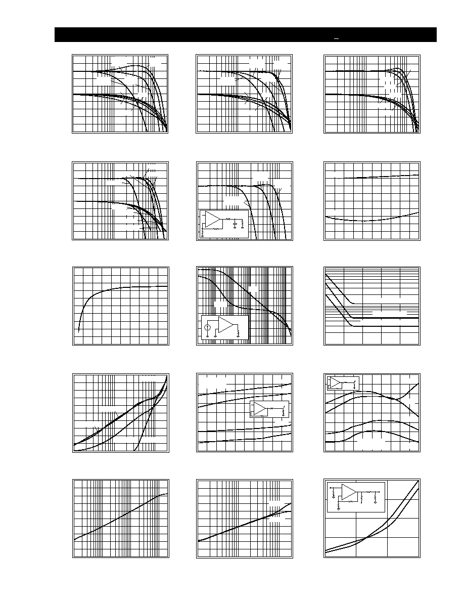
CLC405 Typical Performance Characteristics
(A
V
= +2, R
f
= 348
: V
cc
= + 5V, R
L
= 100
unless specified)
Non-Inverting Frequency Response
Magnitude (1dB/div)
Phase (deg)
-180
-90
-135
-45
0
1
10
100
Frequency (MHz)
Gain
Phase
A
V
+4
A
V
+2
A
V
+2
R
f
=348
A
V
+1
R
f
=2k
A
V
+10
R
f
=100
A
V
+4
R
f
=200
A
V
+10
A
V
+1
Inverting Frequency Response
Magnitude (1dB/div)
Phase (deg)
-360
-270
-315
-225
-180
1
10
100
Frequency (MHz)
Gain
Phase
A
V
-4
A
V
-2
A
V
-4
R
f
=200
A
V
-1
R
f
=348
A
V
-10
R
f
=500
A
V
-10
A
V
-1
A
V
-2
R
f
=200
Frequency Response For Various R
L
s
Magnitude (1dB/div)
Phase (deg)
-180
-90
-135
-45
0
1
10
100
Frequency (MHz)
Gain
Phase
R
L
=50
R
L
=1k
R
L
=100
R
L
=100
R
L
=50
R
L
=1k
Frequency Response vs. V
out
Magnitude (1dB/div)
Phase (deg)
-180
-90
-135
-45
0
1
10
100
Frequency (MHz)
Gain
Phase
V
o
=2V
pp
V
o
=5V
pp
V
o
=0.2V
pp
V
o
=2V
pp
V
o
=1V
pp
V
o
=5V
pp
V
o
=0.2V
pp
V
o
=1V
pp
Frequency Response vs. Capacitive Load
Magnitude (1dB/div)
1
10
100
Frequency (MHz)
C
L
= .001
µ
fd
R
s
=10
C
L
=100pF
R
s
=30
C
L
=10pF
R
s
=100
C
L
1k
R
s
+
-
348
348
Gain Flatness & Linear Phase Deviation
Magnitude (0.1dB/div)
Frequency (MHz)
Phase
Gain
LPD (0.5
o
/div)
0
30
15
Maximum Output Voltage vs. R
L
Maximum Output Voltage (V
pp
)
Load (
)
7.0
6.0
5.0
4.0
3.0
2.0
100
0
200
300
400
500
Open Loop Transimpedance Gain, Z(s)
20 log [|V
o
/|
i
/1
]
1k
10M
100M
Frequency (Hz)
130
110
90
70
50
30
Phase (deg)
200
160
120
80
40
0
Gain
Phase
1M
100k
10k
100
-
+
CLC405
V
o
I
i
Equivalent Input Noise
Noise Voltage (nV/
Hz)
Frequency (Hz)
100
10
1
1k
100
10k
100k
1M
10M
Noise Current (pA/
Hz)
100
10
1
Inverting Current = 12pA/
Hz
Voltage = 5nV/
Hz
Non-Inverting Current = 3pA/
Hz
2nd & 3rd Harmonic Distortion
Distortion (dBc)
Frequency (MHz)
-40
-50
-90
0.1
1
10
-70
-80
-60
3rd R
l
= 100
2nd R
l
= 1k
3rd R
l
= 1k
2nd R
l
= 100
V
o
= 2V
pp
2nd Harmonic Distortion vs. P
out
Distortion (dBc)
Output Power (dBm)
-45
-55
-85
-10
0
10
-65
-75
500KHz
1MHz
5MHz
10MHz
10dBm = 2V
pp
0dBm = .63V
pp
+
-
50
50
P
out
3rd Harmonic Distortion vs. P
out
Distortion (dBc)
Output Power (dBm)
-45
-55
-85
-10
0
10
-65
-75
10dBm = 2V
pp
0dBm = .63V
pp
+
-
50
50
P
out
500KHz
1MHz
5MHz
10MHz
Output Resistance vs. Frequency
Output Resistance (20log Z
out
)
Frequency (MHz)
50
30
1
10
100
-10
-30
10
-50
Forward and Reverse Gain During Disable
Gain (dB)
Frequency (MHz)
0
-20
1
10
100
-60
-80
-40
-100
Forward
Reverse
Differential Gain and Phase
Differential Gain (%)
Differential Phase (deg)
Number of 150
Loads
0.20
0.15
1
2
3
0.05
0
0.10
Gain
Phase
4
1.00
0.75
0.25
0
0.50
75
+
-
348
348
75
CLC405
825
75
V
out
V
in
-V
cc
f = 3.58MHz
3
http://www.national.com

CLC405 Typical Performance Characteristics
(A
V
= +2, R
f
= 348
: V
cc
= + 5V, R
L
= 100
unless specified)
I
BI
, I
BN
, V
IO
vs. Temperature
Offet Voltage, V
IO
(mV)
-60
-20
140
Temperature (
o
C)
V
IO
4.0
3.0
2.0
1.0
0
-1.0
I
BI
, I
BN
(
µ
A)
1.0
0
-1.0
-2.0
-3.0
-4.0
20
60
100
I
BI
I
BN
CLC405 OPERATION
Feedback Resistor
The feedback resistor, R
f
, determines the loop gain and
frequency response for a current feedback amplifier.
Unless otherwise stated, the performance plots and data
sheet specify CLC405 operation with R
f
of 348
at a
gain of +2V/V. Optimize frequency response for different
gains by changing R
f
. Decrease R
f
to peak frequency
response and extend bandwidth. Increase R
f
to roll off
of the frequency response and decrease bandwidth. Use
a 2k
R
f
for unity gain, voltage follower circuits.
Use application note OA-13 to optimize your R
f
selec-
tion. The equations in this note are a good starting
point for selecting R
f
. The value for the inverting input
impedance for OA-13 is approximately 182
.
Enable/Disable Operation Using ± 5V Supplies
The CLC405 has a TTL & CMOS logic compatible
disable function.
Apply a logic low (i.e. < 0.8V) to pin
8, and the CLC405 is guaranteed disabled across its
temperature range. Apply a logic high to pin 8, (i.e. >
2.0V) and the CLC405 is guaranteed enabled. Voltage,
not current, at pin 8 determines the enable/disable
state of the CLC405.
Disable the CLC405 and its inputs and output become
high impedances. While disabled, the CLC405's
quiescent power drops to 8mW.
Use the CLC405's disable to create analog switches or
multiplexers. Implement a single analog switch with one
CLC405 positioned between an input and output.
Create an analog multiplexer with several CLC405s.
Tie the outputs together and put a different signal on
each CLC405 input.
Operate the CLC405 without connecting pin 8.
An
internal 20k
pull-up resistor guarantees the CLC405
is enabled when pin 8 is floating.
Enable/Disable Operation for Single or
Unbalanced Supply Operation
Figure 1
Figure 1 illustrates the internal enable/disable opera-
tion of the CLC405. When pin 8 is left floating or is tied
to +V
cc
, Q1 is on and pulls tail current through the
CLC405 bias circuitry.
When pin 8 is less than
0.8V above the supply midpoint, Q1 stops tail current
from flowing in the CLC405 circuitry. The CLC405 is
now disabled.
Disable Limitations
The feedback resistor, R
f
, limits off isolation in inverting
gain configurations. Do not apply voltages greater than
+V
cc
or less than -V
ee
to pin 8 or any other pin.
Small Signal Pulse Response
Output Voltage
Time (5ns/div)
0.20
0.10
-0.10
-0.20
0.00
A
V
-1
A
V
+1
Large Signal Pulse Response
Output Voltage
Time (5ns/div)
2.0
1.0
-1.0
-2.0
0.0
A
V
-2
A
V
+2
Settling Time vs. Capacitive Load
Settling Time, T
s
(ns) to 0.05% Error
10
100
1000
CL (pF)
C
L
1k
R
s
+
-
348
348
V
o
= 2V step
T
s
R
s
CLC405
50
40
30
20
10
0
R
s
(
)
100
80
60
40
20
0
Short Term Settling Time
V
out
(% Final Value)
Time (ns)
0.2
0.1
-0.1
-0.2
0.0
0
20
100
80
60
40
V
out
= 2Vstep
PSRR and CMRR
PSRR/CMRR (dB)
10k
100k
1M
Frequency (Hz)
10M
100M
60
50
40
30
20
10
PSRR
CMRR
20k
20k
Pin 8
Disable
Q
2
Q
1
Pin 4
-V
ee
20k
Bias
Circuitry
I Tail
Supply
Mid-Point
Pull-up
Resistor
Pin 7
+V
cc
CLC405
NOTE: Pins 4, 7, 8 are external
V
cc
-V
ee
2
http://www.national.com
4

Input - Bias Current, Impedances, and Source
Termination Considerations
The CLC405 has:
∑
a 6M
non-inverting input impedance.
∑
a 100nA non-inverting input bias current.
If a large source impedance application is considered,
remove all parasitic capacitance around the non-invert-
ing input and source traces.
Parasitic capacitances
near the input and source act as a low-pass filter and
reduce bandwidth.
Current feedback op amps have uncorrelated input
bias currents. These uncorrelated bias currents prevent
source impedance matching on each input from can-
celing offsets. Refer to application note OA-07 of the
data book to find specific circuits to correct DC offsets.
Layout Considerations
Whenever questions about layout arise, USE THE
EVALUATION BOARD AS A TEMPLATE.
Use the CLC730013 and CLC730027 evaluation
boards for the DIP and SOIC respectively. These board
layouts were optimized to produce the typical perfor-
mance of the CLC405 shown in the data sheet. To
reduce parasitic capacitances, the ground plane was
removed near pins 2, 3, and 6. To reduce series induc-
tance, trace lengths of components and nodes were
minimized.
Parasitics on traces degrade performance. Minimize
coupling from traces to both power and ground planes.
Use low inductive resistors for leaded components.
Do not use dip sockets for the CLC405 DIP amplifiers.
These sockets can peak the frequency domain
response or create overshoot in the time domain
response.
Use flush-mount socket pins when socket-
ing is necessary.
The 730013 circuit board device
holes are sized for Cambion P/N 450-2598 socket pins
or their functional equivalent.
Insert the back matching resistor (R
out)
shown in Figure
2 when driving coaxial cable or a capacitive load. Use
the plot in the typical performance section labeled
"Settling Time vs. Capacitive Load" to determine the
optimum resistor value for R
out
for different capacitive
loads. This optimal resistance improves settling tim for
pulse-type applications and increases stability.
Figure 2
Use power-supply bypassing capacitors when operat-
ing this amplifier. Choose quality 0.1
µ
F ceramics for C
1
and C
2
. Choose quality 6.8
µ
F tantalum capacitors for
C
3
and C
4
. Place the 0.1
µ
F capacitors within 0.1 inch-
es from the power pins. Place the 6.8
µ
F capacitors
within 3/4 inches from the power pins.
Video Performance vs. I
EX
Improve the video performance of the CLC405 by
drawing extra current from the amplifier output stage.
Using a single external resistor as shown in Figure 3,
you can adjust the differential phase. Video perfor-
mance vs. I
EX
is illustrated below in Graph 1. This graph
represents positive video performance with negative
synchronization pulses.
Graph1
Figure 3
The value for R
pd
in Figure 3 is determined by :
at +5V supplies.
Wideband Digital PGA
As shown on the front page, the CLC405 is easily con-
figured as a digitally controlled programmable gain
amplifier. Make a PGA by configuring several amplifiers
at required gains. Keep R
f
near 348
and change R
g
for each different gain. Use a TTL decoder that has
enough outputs to control the selection of different gains
and the buffer stage. Connect the buffer stage like the
buffer of the front page. The buffer isolates each gain
stage from the load and can produce a gain of zero for
a gain selection of zero. Use of an inverter (7404) on the
buffer disable pin to keep the buffer operational at all
gains except zero. Or float the buffer disable pin for a
continuous enable state.
Differential Gain & Phase vs. I
EX
Differential Gain (%)
I
EX
in mA
0.25
0.20
0.15
0.10
0.05
0
2
0
4
6
8
10
Differential Phase (deg)
0.25
0.20
0.15
0.10
0.05
0
Phase
Gain
12
14
16
18
SMA
Output
SMA
Input
R
in
50
R
f
348
R
out
50
3
7
6
4
2
+5V
-5V
+
+
+
-
R
g
348
C
1
0.1
µ
fd
C
2
0.1
µ
fd
C
3
6.8
µ
fd
C
4
6.8
µ
fd
CLC405
R
pull
down
R
f
R
out
+
-
CLC405
R
g
V
in
-V
cc
R
t
V
out
Extra I
-5V
+5V
R
5
I
pd
EX
=
5
http://www.national.com