 | –≠–ª–µ–∫—Ç—Ä–æ–Ω–Ω—ã–π –∫–æ–º–ø–æ–Ω–µ–Ω—Ç: CLC406A8B | –°–∫–∞—á–∞—Ç—å:  PDF PDF  ZIP ZIP |
CLC410
Fast Settling, Video Op Amp with Disable
General Description
The current-feedback CLC410 is a fast settling, wideband,
monolithic op amp with fast disable/enable feature. De-
signed for low gain applications (A
V
=
±
1 to
±
8), the
CLC410 consumes only 160mW of power (180mW max) yet
provides a -3dB bandwidth of 200MHz (A
V
= +2) and 0.05%
settling in 12ns (15ns max). Plus, the disable feature pro-
vides fast turn on (100ns) and turn off (200ns). In addition,
the CLC410 offers both high performance and stability with-
out compensation - even at a gain of +1.
The CLC410 provides a simple, high performance solution
for video switching and distribution applications, especially
where analog buses benefit from use of the disable function
to "multiplex" signals onto the bus. Differential gain/phase of
0.01%/0.01∞ provide high fidelity and the 60mA output cur-
rent offers ample drive capability.
The CLC410's fast settling, low distortion, and high drive
capabilities make it an ideal ADC driver. The low 160mW
quiescent power consumption and very low 40mW disabled
power consumption suggest use where power is critical
and/or "system off" power consumption must be minimized.
The CLC410 is available in several versions to meet a
variety of requirements. A three letter suffix determines the
version.
Enhanced Solutions (Military/Aerospace)
SMD Number: 5962-90600
Space level versions also available.
For more information, visit http://www.national.com/mil
Features
n
-3dB bandwidth of 200MHz
n
0.05% settling in 12ns
n
Low Power, 160mW (40mW disabled)
n
Low distortion, -60dBc at 20MHz
n
Fast disable (200ns)
n
Differential gain/phase: 0.01%/0.01∞
n
±
1 to
±
8 closed-loop gain range
Applications
n
Video switching and distribution
n
Analog bus driving (with disable)
n
Low power "standby" using Disable
n
Fast, precision A/D conversion
n
D/A current-to-voltage conversion
n
IF processors
n
High speed communications
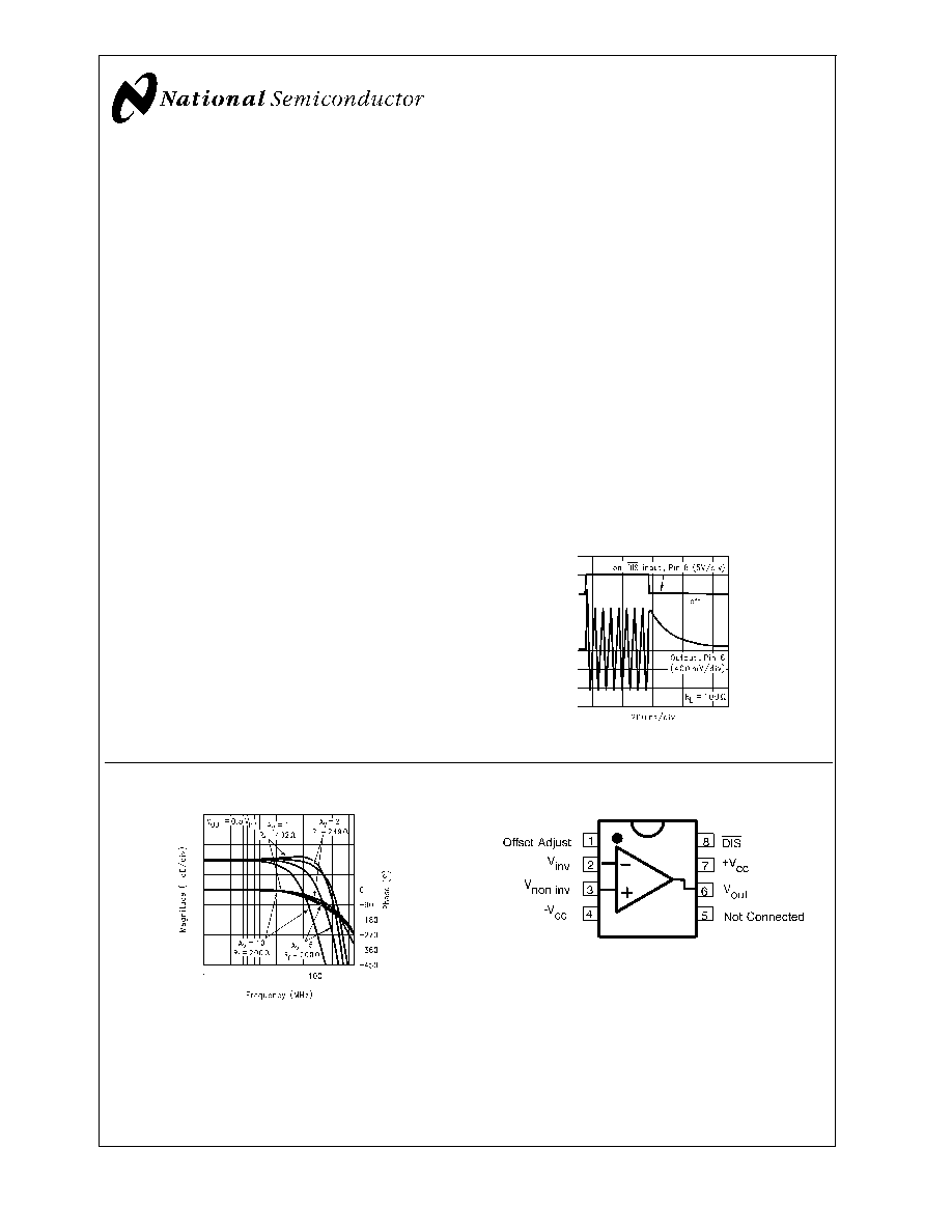
Enable/Disable Response
01274910
Non-Inverting Frequency Response
01274901
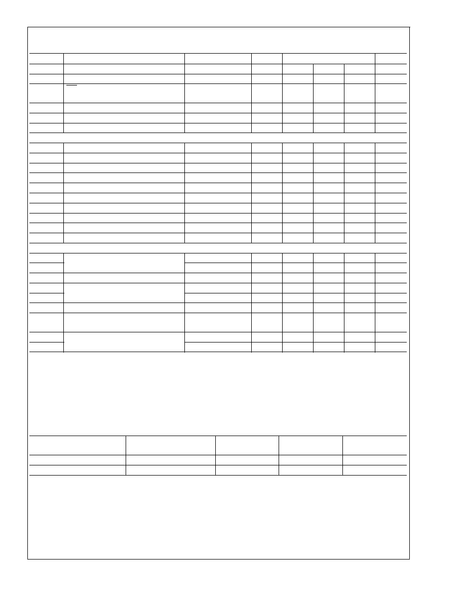
Connection Diagram
01274921
Pinout
DIP & SOIC
July 2001
CLC410
Fast
Settling,
V
ideo
Op
Amp
with
Disable
© 2001 National Semiconductor Corporation
DS012749
www.national.com

Absolute Maximum Ratings
(Note 1)
If Military/Aerospace specified devices are required,
please contact the National Semiconductor Sales Office/
Distributors for availability and specifications.
Supply Voltage (V
CC
)
±
7V
I
OUT
Output is short circuit protected to
ground, but maximum reliability will
be maintained if I
OUT
does not
exceed...
60mA
Common Mode Input Voltage
±
V
CC
Differential Input Voltage
5V
Disable Input Voltage (pin 8)
±
V
CC
-1V
Applied output voltage when
disabled
±
V
CC
Junction Temperature
+150∞C
Operating Temperature Range
-40∞C to +85∞C
Storage Temperature Range
-65∞C to +150∞C
Lead Solder Duration (+300∞C)
10 sec
ESD Rating (human body model)
500V
Operating Ratings
Thermal Resistance
Package
(
JC
)
(
JA
)
MDIP
65∞C/W
120∞C/W
SOIC
60∞C/W
140∞C/W
Electrical Characteristics
A
V
= +2, V
CC
=
±
5V, R
L
= 100
, R
f
= 250
; unless specified
Symbol
Parameter
Conditions
Typ
Max/Min (Note 2)
Units
Ambient Temperature
CLC410AJ
+25∞C
-40∞C
+25∞C
+85∞C
Frequency Domain Response
SSBW
-3dB Bandwidth
V
OUT
<
0.5V
PP
200
>
150
>
150
>
120
MHz
LSBW
V
OUT
<
5V
PP
,
A
V
= +5
50
>
35
>
35
>
35
MHz
Gain Flatness
V
OUT
<
0.5V
PP
GFPL
Peaking
DC to 40MHz
0
<
0.4
<
0.3
<
0.4
dB
GFPH
Peaking
>
40MHz
0
<
0.7
<
0.5
<
0.7
dB
GFR
Rolloff
DC to 75MHz
0.6
<
1
<
1
<
1.3
dB
LPD
Linear Phase Deviation
DC to 75MHz
0.2
<
1
<
1
<
1.2
deg
Time Domain Response
TRS
Rise and Fall Time
0.5V Step
1.6
<
2.4
<
2.4
<
2.4
ns
TRL
5V Step
6.5
<
10
<
10
<
10
ns
TSP
Settling Time to
±
0.1%
2V Step
10
<
13
<
13
<
13
ns
TS
±
0.05%
2V Step
12
<
15
<
15
<
15
ns
OS
Overshoot
0.5V Step
0
<
15
<
10
<
10
%
SR
Slew Rate
A
V
= +2
700
>
430
>
430
>
430
V/µs
SR1
A
V
= -2
1600
≠
≠
≠
V/µs
Distortion And Noise Response
HD2
2nd Harmonic Distortion
2V
PP
, 20MHz
-60
<
-40
<
-45
<
-45
dBc
HD3
3rd harmonic distortion
2V
PP
, 20MHz
-60
<
-50
<
-50
<
-50
dBc
Equivalent Input Noise
SNF
Noise Floor
>
1MHz (Note 4)
-157
<
-154
<
-154
<
-153
dBm
(1Hz)
INV
Integrated Noise
1MHz to 200MHz
(Note 4)
40
<
54
<
57
<
63
µV
DG
Differential Gain (Note 5)
(See Plots)
0.01
0.05
0.04
0.04
%
DP
Differential Phase (Note 5)
(See Plots)
0.01
0.1
0.02
0.02
deg
Disable/Enable Performance
TOFF
Disable Time to
>
50dB
Attenuation at 10MHz
200
<
1000
<
1000
<
1000
ns
TON
Enable Time
100
<
200
<
200
<
200
ns
DIS Voltage
CLC410
www.national.com
2
Electrical Characteristics
(Continued)
A
V
= +2, V
CC
=
±
5V, R
L
= 100
, R
f
= 250
; unless specified
Symbol
Parameter
Conditions
Typ
Max/Min (Note 2)
Units
VDIS
To Disable
1.0
0.5
0.5
0.5
V
VEN
To Enable
2.6
2.3
3.2
4.0
V
DIS current (sourced
from CLC410, see
Figure 5)
IDIS
To Disable
200
250
250
250
µA
IEN
To Enable
80
60
60
60
µA
OSD
Off Isolation
At 10MHz
59
>
55
>
55
>
55
dB
Static, DC Performance
VIO
Input Offset Voltage (Note 3)
2
<
±
8.2
<
±
5.0
<
±
9.0
mV
DVIO
average temperature coefficient
20
<
±
40
≠
<
±
40
µV/∞C
IBN
Input Bias Current (Note 3)
Non Inverting
10
<
±
36
<
±
20
<
±
20
µA
DIBN
Average Temperature Coefficient
100
<
±
200
≠
<
±
100
nA/∞C
IBI
Input Bias Current (Note 3)
Inverting
10
<
±
36
<
±
20
<
±
30
µA
DIBI
Average Temperature Coefficient
50
<
±
200
≠
<
±
100
nA/∞C
PSRR
Power Supply Rejection Ratio
50
>
45
>
45
>
45
dB
CMRR
Common Mode Rejection Ratio
50
>
45
>
45
>
45
dB
ICC
Supply Current (Note 3)
No Load,Quiescent
16
<
18
<
18
<
18
mA
ISD
Supply Current, Disabled
No Load,Quiescent
4
<
6
<
6
<
6
mA
Miscellaneous Performance
RIN
Non-Inverting Input
Resistance
200
>
50
>
100
>
100
k
CIN
Capacitance
0.5
<
2
<
2
<
2
pF
RO
Output Impedance
At DC
0.1
<
0.2
<
0.2
<
0.2
ROD
Output Impedance, Disabled
Resistance,at DC
200
<
100
<
100
<
100
k
COD
Capacitance,at DC
0.5
<
2
<
2
<
2
pF
VO
Output Voltage Range
No Load
±
3.5
>
±
3
>
±
3.2
>
±
3.2
V
CMIR
Common Mode Input Range
For Rated
Performance
±
2.1
>
±
1.2
>
±
2
>
±
2
V
IO
Output Current
-40∞C to +85∞C
±
70
>
±
35
>
±
50
>
±
50
mA
IO
-55∞C to +125∞C
±
60
>
±
30
>
±
50
>
±
50
mA
Note 1: "Absolute Maximum Ratings" are those values beyond which the safety of the device cannot be guaranteed. They are not meant to imply that the devices
should be operated at these limits. The table of "Electrical Characteristics" specifies conditions of device operation.
Note 2: Min/max ratings are based on product characterization and simulation. Individual parameters are tested as noted. Outgoing quality levels are determined
from tested parameters.
Note 3: AJ-level: spec. is 100% tested at +25∞C, sample at 85∞C.
Note 4: Noise tests are performed from 5MHz to 200MHz.
Note 5: Differential gain and phase measured at: A
V
= +2, R
f
= 250
, R
L
= 150
1V
PP
equivalent video signal, 0-100 IRE, 40 IRE
PP
, 3.58 MHz,) IRE =0 volts, at
75
load. See text.
Ordering Information
Package
Temperature Range
Industrial
Part Number
Package
Marking
NSC
Drawing
8-pin plastic DIP
-40∞C to +85∞C
CLC410AJP
CLC410AJP
N08A
8-pin plastic SOIC
-40∞C to +85∞C
CLC410AJE
CLC410AJE
M08A
CLC410
www.national.com
3

Typical Performance Characteristics
(T
A
= 25∞, A
V
= +2, V
CC
=
±
5V, R
L
= 100
; Unless Speci-
fied).
Non-Inverting Frequency Response
Inverting Frequency Response
01274901
01274902
Frequency Response for Various R
L
S
Forward and Reverse Gain During Disable
01274903
01274904
2nd and 3rd Harmonic Distortion
2-Tone, 3rd Order, Intermodulation Intercept
01274905
01274906
CLC410
www.national.com
4

Typical Performance Characteristics
(T
A
= 25∞, A
V
= +2, V
CC
=
±
5V, R
L
= 100
; Unless
Specified). (Continued)
Equivalent Input Noise
CMRR and PSRR
01274907
01274908
Pulse Response
Settling Time
01274928
01274923
Long-Term Settling Time
Settling Time vs. Capacitive Load
01274924
01274909
CLC410
www.national.com
5