
Frequency Response (A
V
= +2V/V)
Features
s
Low-cost
s
High output current: 60mA
s
High input impedance: 6M
s
Gains of +1, +2 with no external components
s
Low power: I
cc
= 3.5mA
s
Ultra-fast enable/disable times
s
Very low input bias currents: 100nA
s
Excellent gain accuracy: 0.1%
s
High speed: 110MHz -3dB BW
Applications
s
Desktop video systems
s
Multiplexers
s
Video distribution
s
Flash A/D driver
s
High-speed switch/driver
s
High-source impedance applications
s
Peak detector circuits
s
Professional video processing
s
High resolution monitors
NOTE: All necessary components are shown.
Typical Application
2:1 Mux Cable Driver
Pinout
DIP & SOIC
General Description
The Comlinear CLC407 is a low-cost, high-speed (110MHz)
buffer which features user-programmable gains of +2, +1, and -1
V/V. This high-performance part has the added versatility of a
TTL-compatible disable which quickly switches the buffer off in
18ns and back on in 40ns. The CLC407's high 60mA output
current, coupled with its ultra-low 35mW power consumption
makes it the ideal choice for demanding applications that are
sensitive to both power and cost.
Utilizing Comlinear's proven architectures, this current feedback
amplifier surpasses the performance of alternate solutions with a
closed-loop design that produces new standards for buffers in
gain accuracy, input impedance, and input bias currents. The
CLC407's internal feedback network provides an excellent gain
accuracy of 0.1%. High source impedance applications will
benefit from the CLC407's 6M
input impedance along with its
exceptionally low 100nA input bias current.
With 0.1dB flatness to 30MHz and low differential gain and phase
errors, the CLC407 is very useful for professional video process-
ing and distribution. A 110MHz -3dB bandwidth coupled with a
350V/
�
s slew rate also make the CLC407 a perfect choice in
cost-sensitive applications such as video monitors, fax machines,
copiers, and CATV systems. Back-terminated video applications
will especially appreciate +2 gains which require no external gain
components reducing inventory costs and board space.
Comlinear CLC407
Low-Cost, Low-Power
Programmable Gain Buffer with Disable
N
August 1996
Comlinear CLC407
Low-Cost, Low-Power
, Programmable Gain Buffer with Disable
� 1996 National Semiconductor Corporation
http://www.national.com
Printed in the U.S.A.
PARAMETERS
CONDITIONS
TYP
MIN/MAX RATINGS
UNITS
NOTES
Ambient Temperature
CLC407AJ
+25�C
+25�C
0 to 70�C
-40 to 85�C
FREQUENCY DOMAIN RESPONSE
-3dB bandwidth
V
out
< 1.0V
pp
110
75
50
45
MHz
B
V
out
< 5.0V
pp
42
31
27
26
MHz
1
�0.1dB bandwidth
V
out
< 1.0V
pp
30
15
MHz
gain flatness
V
out
< 1.0V
pp
peaking
DC to 200MHz
0
0.4
0.6
0.8
dB
B
rolloff
<30MHz
0.1
0.5
0.65
0.7
dB
B
linear phase deviation
<20MHz
0.3
0.6
0.7
0.7
deg
differential gain
NTSC, RL=150
0.03
0.05
0.06
0.07
%
NTSC, RL=150
(Note 2)
0.01
%
2
differential phase
NTSC, RL=150
0.25
0.4
0.5
0.55
deg
NTSC, RL=150
(Note 2)
0.08
deg
2
TIME DOMAIN RESPONSE
rise and fall time
2V step
5
7.5
8.2
8.4
ns
settling time to 0.05%
2V step
18
27
36
39
ns
overshoot
2V step
3
12
12
12
%
slew rate
AV = +2
2V step
350
260
225
215
V/
�
s
AV = -1
1V step
650
V/
�
s
DISTORTION AND NOISE RESPONSE
2nd harmonic distortion
2V
pp
, 1MHz/10MHz
-72/-52
-46
-45
-44
dBc
B, C
3rd harmonic distortion
2V
pp
, 1MHz/10MHz
-70/-57
-50
-47
-46
dBc
B, C
equivalent input noise
non-inverting voltage
>1MHz
5
6.3
6.6
6.7
nV/
Hz
inverting current
>1MHz
12
15
16
17
pA/
Hz
non-inverting current
>1MHz
3
3.8
4
4.2
pA/
Hz
STATIC DC PERFORMANCE
input offset voltage
1
5
7
8
mV
average drift
30
50
50
�
V/�C
input bias current
non-inverting
100
900
1600
2800
nA
A
average drift
3
8
11
nA/�C
input bias current
inverting
1
5
6
8
�
A
average drift
17
40
45
nA/�C
output offset voltage
2.5
13
17
19
mV A,3
amplifier gain error
�0.1%
�1.0%
�1.0%
�1.0%
V/V
A
internal feedback resistor (R
f
)
250
�20%
power supply rejection ratio
DC
52
47
46
45
dB
B
common-mode rejection ratio
DC
50
45
44
43
dB
supply current
R
L
=
3.5
4.0
4.1
4.4
mA
A
disabled
R
L
=
0.8
0.9
0.95
1
mA
A
SWITCHING PERFORMANCE
turn on time
40
55
58
58
ns
turn off time
to >50dB attn. @ 10MHz
18
26
30
32
ns
off isolation
10MHz
85
80
80
80
dB
high input voltage
V
IH
2
2
2
V
low input voltage
V
IL
0.8
0.8
0.8
V
MISCELLANEOUS PERFORMANCE
input resistance
non-inverting
6
3
2.4
1
M
input capacitance
non-inverting
1
2
2
2
pF
common mode input range
�2.2
1.8
1.7
1.5
V
output voltage range
R
L
=
+4.0,-3.3
+3.9,-3.2
+3.8,-3.1
+3.7,-2.8
V
output current
60
44
38
20
mA
output resistance, closed loop
0.06
0.2
0.25
0.4
Recommended gain range +1, +2 V/V
Min/max ratings are based on product characterization and simulation. Individual parameters are tested as noted. Outgoing quality levels are
determined from tested parameters.
CLC407 Electrical Characteristics
(A
V
= +2, V
cc
= + 5V, R
L
= 100
unless specified)
Absolute Maximum Ratings
supply voltage
�7V
I
out
is short circuit protected to ground
common-mode input voltage
�Vcc
maximum junction temperature
+175�C
storage temperature range
-65�C to +150�C
lead temperature (soldering 10 sec)
+300�C
Notes
1) At temps < 0�C, spec is guaranteed for R
L
= 500
.
2) An 825
pull-down resistor is connected between V
o
and -V
cc
.
3) Source impedance 1k
.
A) J-level: spec is 100% tested at +25�C, sample tested at +85�C.
LC/MC-level: spec is 100% wafer probed at +25�C.
B) J-level: spec is sample tested at +25�C.
C) Guaranteed at 10MHz.
http://www.national.com
2
CLC407 Typical Performance Characteristics
(A
V
= +2, R
f
= 250
: V
cc
= + 5V, R
L
= 100
unless specified)
Frequency Response
Magnitude (1dB/div)
Phase (45
o
/div)
1
10
100
Frequency (MHz)
Gain
Phase
A
V
+2
A
V
+1
A
V
+1
A
V
-1
A
V
+2
A
V
-1
Frequency Response vs. R
L
Magnitude (1dB/div)
Phase (deg)
-180
-90
-135
-45
0
1
10
100
Frequency (MHz)
Gain
Phase
R
L
=50
R
L
=100
R
L
=1k
R
L
=50
R
L
=100
R
L
=1k
Frequency Response vs. V
out
(A
v
= +2)
Magnitude (1dB/div)
Phase (deg)
-180
-90
-135
-45
0
1
10
100
Frequency (MHz)
Gain
Phase
V
O
=1V
pp
V
O
=0.2V
pp
V
O
=5V
pp
V
O
=2V
pp
V
O
=5V
pp
V
O
=0.2V
pp
V
O
=1V
pp
V
O
=2V
pp
Frequency Response vs. V
out
(A
v
= +1)
Magnitude (1dB/div)
Phase (deg)
-180
-90
-135
-45
0
1
10
100
Frequency (MHz)
Gain
Phase
V
O
=1V
pp
V
O
=0.2V
pp
V
O
=2V
pp
V
O
=4V
pp
V
O
=2V
pp
V
O
=4V
pp
V
O
=1V
pp
V
O
=0.2V
pp
Frequency Response vs. V
out
(A
v
= -1)
Magnitude (1dB/div)
Phase (deg)
-360
-270
-315
-225
-180
1
10
100
Frequency (MHz)
Gain
Phase
V
O
=1V
pp
V
O
=0.2V
pp
V
O
=2V
pp
V
O
=4V
pp
V
O
=2V
pp
V
O
=4V
pp
V
O
=1V
pp
V
O
=0.2V
pp
Frequency Response vs. Capacitive Load
Magnitude (1dB/div)
Phase (deg)
-180
-90
-135
-45
0
1
10
100
Frequency (MHz)
Gain
Phase
C
L
=1kpF
R
s
=10
C
L
=100pF
R
s
= 30
C
L
=10pF
R
s
=100
C
L
=1kpF
C
L
=100pF
C
L
=10pF
Maximum Output Voltage vs. R
L
Maximum Output Voltage (V
pp
)
Load (
)
7.0
6.0
5.0
4.0
3.0
2.0
100
0
200
300
400
500
Gain Flatness & Linear Phase Deviation
Magnitude (0.1dB/div)
LPD (0.5
o
/div)
0
15
30
Frequency (MHz)
Gain
Phase
Equivalent Input Noise
Noise Voltage (nV/
Hz)
Frequency (Hz)
100
10
1
1k
100
10k
100k
1M
10M
Noise Current (pA/
Hz)
100
10
1
Inverting Current = 12pA/
Hz
Voltage = 5nV/
Hz
Non-Inverting Current = 3pA/
Hz
2nd & 3rd Harmonic Distortion
Distortion (dBc)
Frequency (MHz)
-40
-50
-90
0.1
1
10
-70
-80
-60
3rd R
l
= 100
2nd R
l
= 1k
3rd R
l
= 1k
2nd R
l
= 100
V
o
= 2V
pp
2nd Harmonic Distortion vs. P
out
Distortion (dBc)
Output Power (dBm)
-45
-55
-85
-10
0
10
-65
-75
500KHz
1MHz
5MHz
10MHz
10dBm = 2V
pp
0dBm = .63V
pp
+
-
50
50
P
out
3rd Harmonic Distortion vs. P
out
Distortion (dBc)
Output Power (dBm)
-45
-55
-85
-10
0
10
-65
-75
10dBm = 2V
pp
0dBm = .63V
pp
+
-
50
50
P
out
500KHz
1MHz
5MHz
10MHz
Output Resistance vs. Frequency
Output Resistance (20log Z
out
)
Frequency (MHz)
50
30
1
10
100
-10
-30
10
-50
Forward & Reverse Isolation During Disable
Gain (dB)
1
10
100
Frequency (MHz)
Forward
Reverse
-20
-40
-60
-80
-100
-120
Differential Gain & Phase
Differential Gain (%)
1
2
4
Number of 150
Loads
0.20
0.15
0.10
0.05
0
Differential Phase (deg)
1.00
0.75
0.50
0.25
0
Phase
Gain
3
3
http://www.national.com
Closed Loop Gain Selection
The CLC407 is a current feedback op amp with
R
f
= R
g
= 250
on chip (in the package). Select from
three closed loop gains without using any external gain or
feedback resistors. Implement gains of +2, +1, and
-1V/V by connecting pins 2 and 3 as described in the
chart below.
The gain accuracy of the CLC407 is excellent and
stable over temperature change. The internal gain
setting resistors, R
f
and R
g
are diffused silicon resistors
with a process variation of � 20% and a temperature
coefficient of ~ 2000ppm/�C. Although their absolute
values change with processing and temperature, their
ratio (R
f
/R
g
) remains constant. If an external resistor is
used in series with R
g
, gain accuracy over temperature
will suffer .
Non-Inverting Unity Gain Considerations (A
v
= +1V/V)
Achieve a gain of +1V/V by removing all resistive and
capacitive connections between pin 2 and ground plane.
Any capacitive coupling between pin 2 and ground will
cause high frequency peaking in the frequency domain
response and overshoot in the time domain response.
Minimize this capacitive coupling during layout by removing
ground plane near pins 1, 2, and 3. This minimization
should produce a response similar to the plot labeled
"open" in Graph 1. If desired flatness is greater than plot
"open" in Graph 1, two options remain to further flatten
the frequency response. First, try shorting the inverting
input (pin 2) to the non-inverting input (pin 3). This
response is labeled "short" in Graph 1. Next, try
inserting a 300
resistor R between the non-inverting
input (pin 2) as shown in Figure 1. This response is
labeled "300
" in Graph 1. Notice an "open" produces a
response with obvious peaking and maximum bandwidth,
a "short" minimizes peaking and bandwidth, and finally
300
slightly extends bandwidth with minimal peaking.
Graph 1
Gain
Input Connections
Acl
Non-Inverting (pin3)
Inverting (pin2)
-1V/V
ground
input signal
+1V/V
input signal
NC (open)
+2V/V
input signal
ground
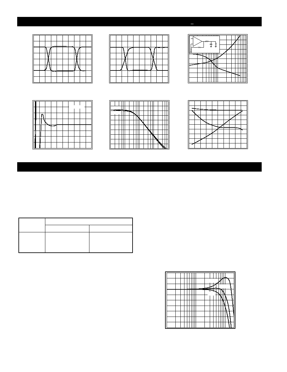
CLC407 Typical Performance Characteristics
(A
V
= +2, R
f
= 250
: V
cc
= + 5V, R
L
= 100
unless specified)
I
BI
, I
BN
, V
IO
vs. Temperature
Offet Voltage, V
IO
(mV)
-60
-20
140
Temperature (
o
C)
V
IO
4.0
3.0
2.0
1.0
0
-1.0
I
BI
, I
BN
(
�
A)
1.0
0
-1.0
-2.0
-3.0
-4.0
20
60
100
I
BI
I
BN
CLC407 OPERATION
Small Signal Pulse Response
Output Voltage
Time (5ns/div)
0.20
0.10
-0.10
-0.20
0.00
A
V
-1
A
V
+2
Large Signal Pulse Response
Output Voltage
Time (5ns/div)
2.0
1.0
-1.0
-2.0
0.0
A
V
-1
A
V
+2
Settling Time vs. Capacitive Load
Settling Time, T
s
(ns) to 0.05% Error
10
100
1000
C
L
(pF)
C
L
1k
R
s
+
-
250
250
V
o
= 2V step
T
s
R
s
CLC407
50
40
30
20
10
0
R
s
(
)
100
80
60
40
20
0
Short Term Settling Time
V
out
(% Final Value)
Time (ns)
0.2
0.1
-0.1
-0.2
0.0
0
20
100
80
60
40
V
out
= 2Vstep
PSRR and CMRR
PSRR/CMRR (dB)
10k
100k
1M
Frequency (Hz)
10M
100M
60
50
40
30
20
10
PSRR
CMRR
Frequency Response vs.
Unity Gain Configuration
Magnitude (1dB/div)
Frequency (MHz)
1
10
100
Short
300
Open
http://www.national.com
4
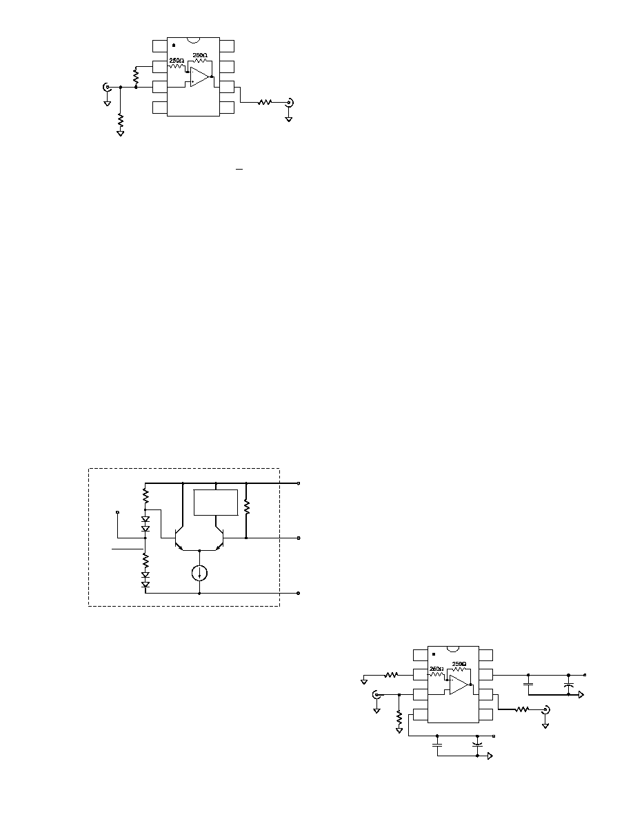
Figure 1
Enable/Disable Operation Using +5V Supplies
The CLC407 has a TTL & CMOS logic compatible
disable function. Apply a logic low (i.e. < 0.8V) to pin
8, and the CLC407 is guaranteed disabled across its
temperature range. Apply a logic high to pin 8, (i.e. >
2.0V) and the CLC407 is guaranteed enabled. Voltage,
not current, at pin 8 determines the enable/disable
state of the CLC407.
Disable the CLC407 and its inputs and output become
high impedances. While disabled, the CLC407's quies-
cent power drops to 8mW.
Use the CLC407's disable to create analog switches or
multiplexers. Implement a single analog switch with
one CLC407 positioned between an input and output.
Create an analog multiplexer with several CLC407s.
Tie the outputs together and put a different signal on
each CLC407 input.
Operate the CLC407 without connecting pin 8. An
internal 20k
pull-up resistor guarantees the CLC407
is enabled when pin 8 is floating.
Enable/Disable Operation for Single or
Unbalanced Supply Operation
Figure 2
Figure 2 illustrates the internal enable/disable
operation of the CLC407. When pin 8 is left floating or
is tied to +V
cc
, Q
1
is on and pulls tail current through
the CLC407 circuitry. When pin 8 is less than 0.8V
above the supply mid-point, Q
1
stops tail current from
flowing in the bias circuitry. The CLC407 is now disabled.
Disable Limitations
The internal feedback resistor, R
f
limits off isolation in
inverting gain configurations. Do not apply voltages
greater than +V
cc
or less than -V
ee
to pin 8.
Input - Bias Current, Impedances, and Source
Termination Considerations
The CLC407 has:
�
a 6M
non-inverting input impedance.
�
100nA non-inverting input bias current.
If a large source impedance application is considered,
remove all parasitic capacitance around the non-invert-
ing input and source traces. Parasitic capacitances
near the input and source act as a low-pass filter and
reduce bandwidth.
Current feedback op amps have uncorrelated input
bias currents. These uncorrelated bias currents
prevent source impedance matching on each input
from cancelling offsets. Refer to application note
OA-07 of the data book to find specific circuits to
correct DC offsets.
Layout Considerations
Whenever questions about layout arise, USE THE
EVALUATION BOARD AS A TEMPLATE.
Use the 730013 and 730026 evaluation boards for the
DIP and SOIC respectively. These board layouts were
optimized to produce the typical performance of the
CLC407 shown in the data sheet. To reduce parasitic
capacitances, the ground plane was removed near
pins 2, 3, and 6. To reduce series inductance, trace
lengths of components and nodes were minimized.
Parasitics on traces degrade performance. Minimize
coupling from traces to both power and ground
planes. Use low inductance resistors for leaded
components .
Do not use dip sockets for the CLC407 DIP amplifiers.
These sockets can peak the frequency domain
response or create overshoot in the time domain
response. Use flush-mount socket pins if socketing
cannot be avoided. The 730013 circuit board device
holes are sized for Cambion P/N 450-2598 socket pins
or their functional equivalent.
Insert the back matching resistor R
out
shown in
Figure 3 when driving coaxial cable or a capacitive
load. Use the plot in the typical performance section
labeled "Settling Time vs. Capacitive Load" to determine
the optimum resistor value for R
out
for different capac-
itive loads. This optimal resistance improves settling
time for pulse-type applications and increases stability.
Figure 3
SMA
Output
SMA
Input
R
in
50
R
out
50
+5V
-5V
+
+
C
1
0.1
�
fd
C
2
0.1
�
fd
C
3
6.8
�
fd
C
4
6.8
�
fd
J
1
= 0
1
CLC407
7
6
8
5
3
4
2
20k
20k
Pin 8
Disable
Q
2
Q
1
Pin 4
-V
ee
20k
Bias
Circuitry
I Tail
Supply
Mid-Point
Pull-up
Resistor
Pin 7
+V
cc
CLC407
NOTE: Pins 4, 7, 8 are external
V
cc
-V
ee
2
SMA
Output
SMA
Input
R
in
50
R
out
50
R
1
CLC407
7
6
8
5
3
4
2
5
http://www.national.com