 | –≠–ª–µ–∫—Ç—Ä–æ–Ω–Ω—ã–π –∫–æ–º–ø–æ–Ω–µ–Ω—Ç: CLC408 | –°–∫–∞—á–∞—Ç—å:  PDF PDF  ZIP ZIP |

Features
s
96mA output current
s
1.5mA supply current
s
130MHz bandwidth (Av = +2)
s
-85/-75dBc HD2/HD3 (1MHz)
s
15ns settling to 0.2%
s
350V/
µ
s slew rate
s
Dual version available (CLC418)
Applications
s
Coaxial cable driver
s
Twisted pair driver
s
Transformer/coil driver
s
High capacitive load driver
s
Video line driver
s
ADSL/HDSL driver
s
Portable/battery-powered line driver
s
A/D driver
V
EE
R
f1
+
-
CLC408
R
t1
Z
0
R
f2
-
+
CLC426
V
inA
R
g2
R
t2
R
m1
V
oB
R
f1
+
-
CLC408
R
t1
R
f2
-
+
CLC426
V
inB
R
g2
R
t2
R
m1
V
oA
Typical Application Diagram
Full Duplex Cable Driver
Pinout
DIP & SOIC
General Description
The Comlinear CLC408 delivers high output drive current
(96mA), but consumes minimal quiescent supply current
(1.5mA). Its current feedback architecture, fabricated in an
advanced complementary bipolar process, maintains consistent
performance over a wide range of gains and signal levels.
The CLC408 offers superior dynamic performance with a
130MHz small-signal bandwidth, 350V/
µ
s slew rate and 4.6ns
rise/fall times (2V
pp
). The combination of low quiescent power,
high output drive current, and high-speed performance make
the CLC408 a great choice for many portable and battery-
powered personal communication and computing systems.
The CLC408 drives low-impedance loads, including capacitive
loads, with little change in performance. Into a 100
load, it
delivers -85/-64dBc second/third harmonic distortion (A
v
= +2,
V
o
= 2V
pp
, f = 1MHz). With a 25
load, and the same
conditions, it produces only -67/-62dBc second/third harmonic
distortion. It is also an excellent choice for driving high currents
into single-ended transformers and coils.
When driving the input of high resolution A/D converters, the
CLC408 provides excellent -85/-75dBc second/third harmonic
distortion and fast settling time (A
v
= +2, V
o
= 2V
pp
, f = 1MHz,
R
L
=1k
).
Non-Inverting Frequency Response
(A
v
= +2V/V, R
L
= 25
)
Normalized Magnitude (1dB/div)
Frequency (Hz)
10M
1M
100M
Comlinear CLC408
High-Speed, Low-Power Line Driver
N
August 1996
Comlinear CLC408
High-Speed, Low-Power Line Driver
© 1996 National Semiconductor Corporation
http://www.national.com
Printed in the U.S.A.
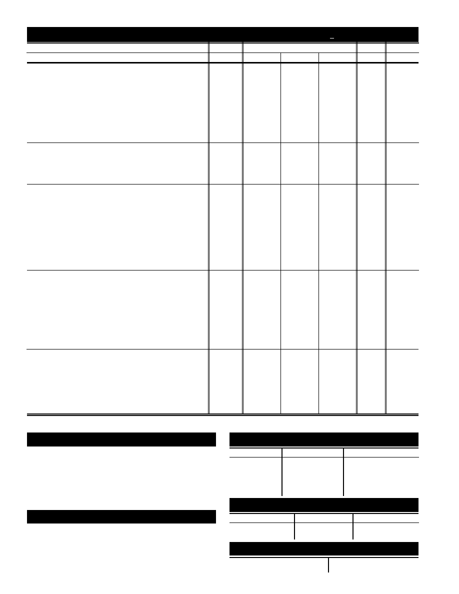
PARAMETERS
CONDITIONS
TYP
MIN/MAX RATINGS
UNITS
NOTES
Ambient Temperature
CLC408AJ
+25∞C
+25∞C
0 to 70∞C
-40 to 85∞C
FREQUENCY DOMAIN RESPONSE
-3dB bandwidth
V
out
< 1.0V
pp
130
90
80
75
MHz
B
V
out
< 4.0V
pp
45
33
29
28
MHz
-0.1dB bandwidth
V
out
< 1.0V
pp
60
30
25
25
MHz
gain flatness
V
out
< 1.0V
pp
peaking
DC to 200MHz
0.1
0.5
0.9
1.0
dB
B
rolloff
<30MHz
0
0.1
0.25
0.25
dB
B
linear phase deviation
<30MHz
0.2
0.4
0.5
0.5
deg
differential gain
NTSC, R
L
=150
0.1
≠
≠
≠
%
differential phase
NTSC, R
L
=150
0.4
≠
≠
≠
deg
TIME DOMAIN RESPONSE
rise and fall time
2V step
4.6
7.0
7.5
8.0
ns
settling time to 0.2%
2V step
15
30
38
40
ns
overshoot
2V step
5
12
12
12
%
slew rate
A
V
= +2
2V step
350
260
225
215
V/
µ
s
DISTORTION AND NOISE RESPONSE
2
nd
harmonic distortion
2V
pp
, 1MHz
-85
≠
≠
≠
dBc
2V
pp
, 1MHz; RL = 1k
-85
≠
≠
≠
dBc
2V
pp
, 5MHz
-65
-60
-58
-58
dBc
B
3
rd
harmonic distortion
2V
pp
, 1MHz
-64
≠
≠
≠
dBc
2V
pp
, 1MHz; RL = 1k
-75
≠
≠
≠
dBc
2V
pp
, 5MHz
-50
-45
-44
-44
dBc
B
equivalent input noise
voltage (e
ni
)
>1MHz
5
6.3
6.6
6.7
nV/
Hz
non-inverting current (i
bn
)
>1MHz
1.4
1.8
1.9
2.3
pA/
Hz
inverting current (i
bi
)
>1MHz
13
16
17
18
pA/
Hz
STATIC DC PERFORMANCE
input offset voltage
2
8
11
11
mV
A
average drift
25
≠
35
40
µ
V/∞C
input bias current (non-inverting)
2
8
11
15
µ
A
A
average drift
60
≠
80
110
nA/∞C
input bias current (inverting)
2
10
18
20
µ
A
A
average drift
20
≠
90
110
nA/∞C
power supply rejection ratio
DC
55
50
48
48
dB
B
common-mode rejection ratio
DC
52
48
46
46
dB
supply current
R
L
=
1.5
1.7
1.8
1.8
mA
A
MISCELLANEOUS PERFORMANCE
input resistance (non-inverting)
5
3
2.5
1
M
input capacitance (non-inverting)
1
2
2
2
pF
common mode input range
±2.7
±2.3
±2.2
±2.0
V
output voltage range
R
L
= 100
± 3.3
±2.9
±2.8
±2.6
V
output voltage range
R
L
=
±4.0
±3.8
±3.7
±3.5
V
output current
96
96
96
60
mA
C
output resistance, closed loop
DC
0.03
0.15
0.2
0.3
CLC408 Electrical Characteristics
(A
v
= +2, R
f
= 1k
, R
L
= 100
, V
CC
= + 5V, unless specified)
Absolute Maximum Ratings
supply voltage
±7V
output current (see note C)
96mA
common-mode input voltage
±V
CC
maximum junction temperature
+175∞C
storage temperature range
-65∞C to +150∞C
lead temperature (soldering 10 sec)
+300∞C
ESD rating (human body model)
2000V
Notes
A) J-level: spec is 100% tested at +25∞C, sample tested at +85∞C.
LC/MC-level: spec is 100% wafer probed at +25∞C.
B) J-level: spec is sample tested at +25∞C.
C) The output current sourced or sunk by the CLC408 can
exceed the maximum safe output current.
Ordering Information
Model
Temperature Range
Description
CLC408AJP
-40
∞
C to +85
∞
C
8-pin PDIP
CLC408AJE
-40
∞
C to +85
∞
C
8-pin SOIC
CLC408AJE-TR
-40
∞
C to +85
∞
C
8-pin SOIC, 750pc reel
CLC408AJE-TR13
-55
∞
C to +125
∞
C
8-pin SOIC, 2500pc reel
CLC408ALC
-40
∞
C to +85
∞
C
dice (commercial)
Package Thermal Resistance
Package
q
JC
q
JA
Plastic (AJP)
115
∞
C/W
125
∞
C/W
Surface Mount (AJE)
130
∞
C/W
150
∞
C/W
Reliability Information
Transistor Count
38
MTBF (based on limited test data)
46Mhr
Min/max ratings are based on product characterization and simulation. Individual parameters are tested as noted. Outgoing quality levels are
determined from tested parameters.
http://www.national.com
2
3
http://www.national.com
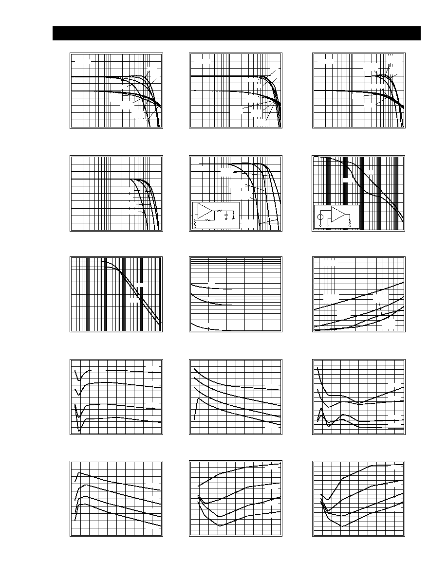
Typical Performance Characteristics
(A
v
= +2, R
f
= 1k
, R
L
= 100
,
V
CC
= +5V, T = 25∞C, CLC408AJ
;
unless specified)
Non-Inverting Frequency Response
Normalized Magnitude (1dB/div)
Frequency (Hz)
10M
Phase (deg)
-90
-180
-450
-270
-360
1M
100M
A
v
+1
A
v
+2
R
f
=953
A
v
+2
A
v
+5
R
f
=402
A
v
+5
A
v
+10
R
f
=200
A
v
+10
A
v
+1
R
f
=3k
0
V
o
= 1V
pp
Gain
Phase
Inverting Frequency Response
Normalized Magnitude (1dB/div)
Frequency (Hz)
10M
Phase (deg)
0
-270
-360
-450
-90
-180
1M
100M
A
v
-1
A
v
-2
R
f
=681
A
v
-2
A
v
-5
R
f
=301
A
v
-5
A
v
-10
R
f
=200
A
v
-10
A
v
-1
R
f
=806
Gain
Phase
V
o
= 1V
pp
Frequency Response vs. R
L
Normalized Magnitude (1dB/div)
Frequency (Hz)
10M
Phase (deg)
-90
-180
-450
-270
-360
1M
100M
R
L
=1k
R
f
=1.21k
R
L
=25
R
L
=100
R
L
=100
R
f
=1k
R
L
=1k
R
L
=25
R
f
=0.95k
0
Gain
Phase
V
o
= 1V
pp
Frequency Response vs. V
out
Normalized Magnitude (1dB/div)
Frequency (Hz)
10M
1M
100M
0.10V
pp
2.0V
pp
4.0V
pp
1.0V
pp
Frequency Response vs. Capacitive Load
Magnitude (1dB/div)
Frequency (Hz)
10M
1M
100M
C
L
=100pF
R
s
=24.9
C
L
=10pF
R
s
=100
C
L
= 1000pF
R
s
=5.7
C
L
1k
R
s
+
-
1k
1k
C
L
=0pF
R
s
=0
V
o
= 1V
pp
Open Loop Transimpedance Gain, Z(s)
20 logIZI (dB
)
Frequency (Hz)
120
100
40
1k
10k
100M
80
60
Gain
Phase (deg)
180
140
20
100
60
Phase
100k
1M
10M
100
-
+
CLC408
V
o
I
i
PSRR and CMRR
PSRR/CMRR (dB)
Frequency (Hz)
60
50
20
10
0
1k
10k
100k
40
30
CMRR
1M
10M
100M
PSRR
Equivalent Input Noise
Noise Voltage (nV/
Hz)
Frequency (Hz)
100
1
1k
10k
100M
10
i
bi
Noise Current (pA/
Hz)
100
10
1
100k
1M
10M
e
ni
i
bn
2nd & 3rd Harmonic Distortion
Distortion (dBc)
Frequency (Hz)
-50
-40
-30
-20
-60
-90
1M
10M
-70
-80
2nd
R
L
= 1k
3rd
R
L
= 100
3rd
R
L
= 1k
2nd
R
L
= 100
V
o
= 2V
pp
2nd Harmonic Distortion, R
L
= 25
Distortion (dBc)
Output Amplitude (V
pp
)
-55
-50
-45
-60
-75
0
1
5
-65
-70
1MHz
2
3
4
2MHz
5MHz
10MHz
3rd Harmonic Distortion, R
L
= 25
Distortion (dBc)
Output Amplitude (V
pp
)
-40
-30
-20
-50
-80
0
1
5
-60
-70
1MHz
2
3
4
2MHz
5MHz
10MHz
2nd Harmonic Distortion, R
L
= 100
Distortion (dBc)
Output Amplitude (V
pp
)
-90
-85
-80
-75
-70
-65
-60
-55
-50
0
1
5
1MHz
2
3
4
2MHz
5MHz
10MHz
3rd Harmonic Distortion, R
L
= 100
Distortion (dBc)
Output Amplitude (V
pp
)
-80
-70
-60
-50
-40
-30
0
1
5
1MHz
2
3
4
2MHz
5MHz
10MHz
2nd Harmonic Distortion, R
L
= 1k
Distortion (dBc)
Output Amplitude (V
pp
)
-95
-90
-85
-80
-75
-70
-65
-60
0
1
5
1MHz
2
3
4
2MHz
5MHz
10MHz
3rd Harmonic Distortion, R
L
= 1k
Distortion (dBc)
Output Amplitude (V
pp
)
-95
-90
-85
-80
-75
-70
-65
-60
-55
0
1
5
1MHz
2
3
4
2MHz
5MHz
10MHz
http://www.national.com
4
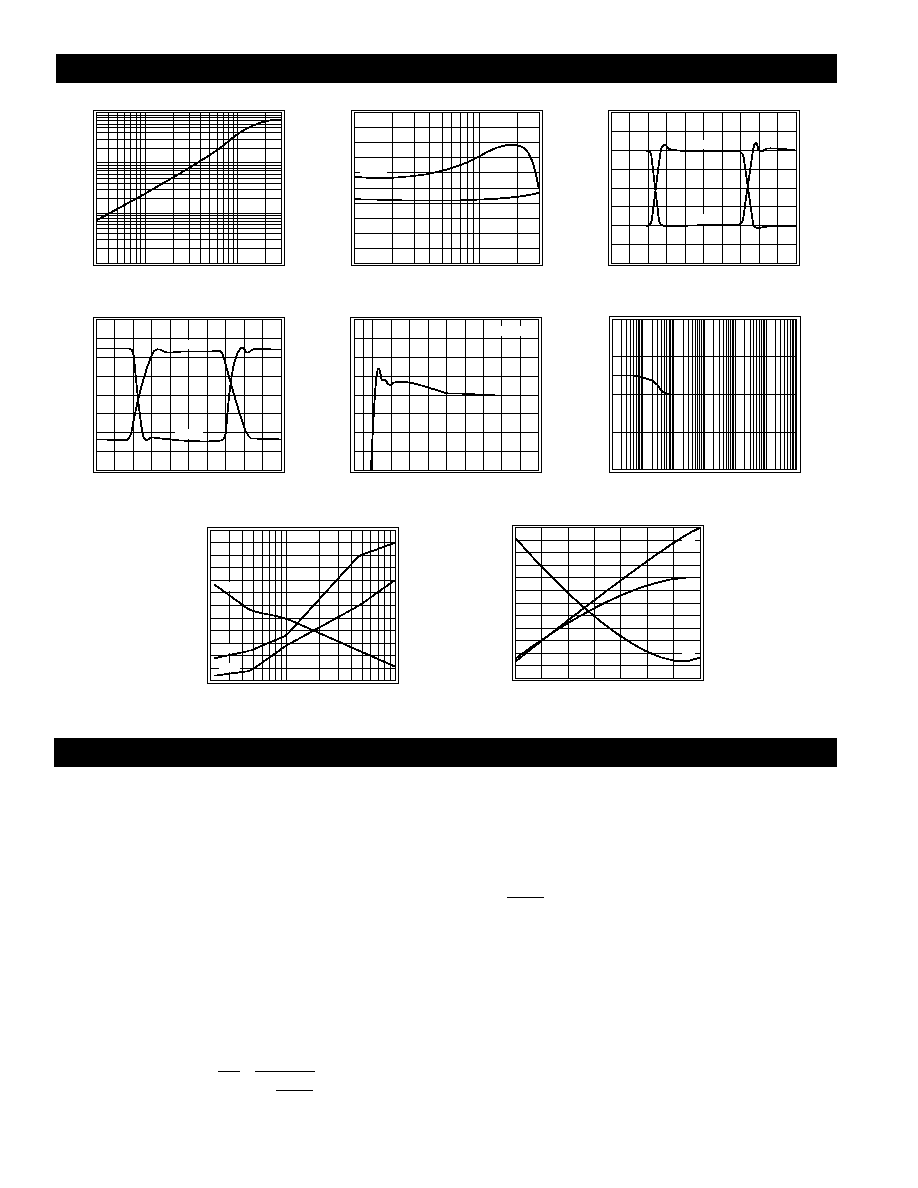
Typical Performance Characteristics
(A
v
= +2, R
f
= 1k
, R
L
= 100
,
V
CC
= +5V, T = 25∞C, CLC408AJ
;
unless specified)
Long Term Settling Time
V
o
(% Output Step)
Time (s)
0.4
-0.4
1
µ
1m
1
0
10
µ
100
µ
10m
100m
-0.2
0.2
Closed Loop Output Resistance
Output Resistance (
)
Frequency (Hz)
100
0.1
10M
100M
10
1
Gain Flatness & Linear Phase Deviation
Magnitude (0.1dB/div)
Frequency (Hz)
1M
10M
Gain
Phase Deviation (0.1
∞
/div)
Phase
Small Signal Pulse Response
Output Voltage
Time (10ns/div)
0.20
0.10
-0.20
0
-0.10
A
v
+2
A
v
-2
Large Signal Pulse Response
Output Voltage
Time (10ns/div)
4.0
2.0
-4.0
0
-2.0
A
v
+2
A
v
-2
Short Term Settling Time
V
o
(% Output Step)
Time (s)
0.2
0.1
-0.2
0
20n
100n
0
-0.1
V
out
= 2V
step
40n
60n
80n
I
BI
, I
BN
, V
OS
vs. Temperature
Offset Voltage V
OS
(mV)
Temperature (
∞
C)
7.0
6.0
1.0
-50
0
100
5.0
4.0
3.0
2.0
V
OS
I
BI
, I
BN
(
µ
A)
3.5
3.0
1.5
1.0
0.5
2.5
2.0
50
I
BI
I
BN
Settling Time vs. Capacitive Load
Settling Time (ns)
CL (F)
70
60
30
20
10
100p
20p
1000p
50
40
Rs (
)
60
50
20
10
0
40
30
R
s
0.05%
0.1%
CLC408 OPERATION
The CLC408 has a current-feedback (CFB) architecture
built in an advanced complementary bipolar process.
The key features of current-feedback are:
s
AC bandwidth is independent of voltage gain
s
Inherently unity-gain stability
s
Frequency response may be adjusted with
feedback resistor (R
f
in Figures 1-3)
s
High slew rate
s
Low variation in performance for a wide range
of gains, signal levels and loads
s
Fast settling
Current-feedback operation can be explained with a
simple model. The voltage gain for the circuits in Figures 1
and 2 is approximately:
where:
s
A
v
is the DC voltage gain
s
R
f
is the feedback resistor
s
Z(j
) is the CLC408's open-loop
transimpedance gain
s
is the loop gain
The denominator of the equation above is approximately
1 at low frequencies. Near the -3dB corner
frequency, the interaction between R
f
and Z(j
)
dominates the circuit performance. Increasing R
f
does
the following:
s
Decreases loop gain
s
Decreases bandwidth
s
Reduces gain peaking
s
Lowers pulse response overshoot
s
Affects frequency response phase linearity
V
V
A
1
R
Z j
o
in
v
f
=
+
( )
Z j
R
f
( )
5
http://www.national.com
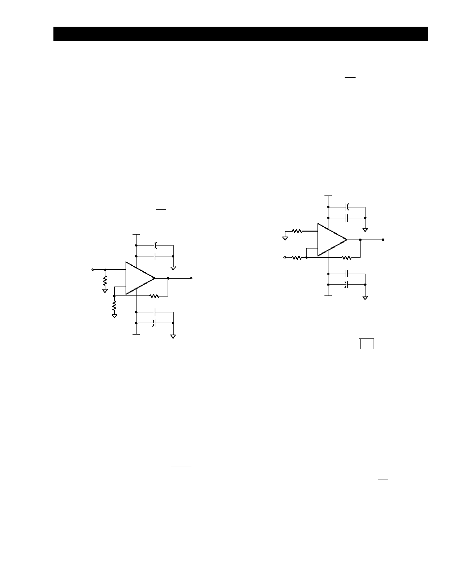
CLC408 DESIGN INFORMATION
Standard op amp circuits work with CFB op amps.
There are 3 unique design considerations for CFB:
s
The feedback resistor (R
f
in Figures 1-3) sets
AC performance
s
R
f
cannot be replaced with a short or a capacitor
s
The output offset voltage is not reduced by
balancing input resistances
The following sub-sections cover:
s
Design parameters, formulas and techniques
s
Interfaces
s
Application circuits
s
Layout techniques
s
SPICE model information
DC Gain (non-inverting)
The non-inverting DC voltage gain for the configuration
shown in Figure 1 is:
Figure 1: Non-Inverting Gain
The normalized gain plots in the
Typical Performance
Characteristics section show different feedback
resistors (R
f
) for different gains. These values of R
f
are
recommended for obtaining the highest bandwidth with
minimal peaking. The resistor R
t
provides DC bias for
the non-inverting input.
For A
v
< 6, use linear interpolation on the nearest A
v
values to calculate the recommended value of R
f
. For
A
v
6, the minimum recommended R
f
is 200
.
Select R
g
to set the DC gain:
DC gain accuracy is usually limited by the tolerance of
R
f
and R
g
.
DC Gain (unity gain buffer)
The recommended R
f
for unity gain buffers is 3k
. R
g
is left open. Parasitic capacitance at the inverting node
may require a slight increase of R
f
to maintain a flat
frequency response.
DC Gain (inverting)
The inverting DC voltage gain for the configuration
shown in Figure 2 is:
The normalized gain plots in the
Typical Performance
Characteristics section show different feedback
resistors (R
f
) for different gains. These values of R
f
are
recommended for obtaining the highest bandwidth with
minimal peaking. The resistor R
t
provides DC bias for
the non-inverting input.
For |A
v
| < 6, use linear interpolation on the nearest A
v
values to calculate the recommended value of R
f
. For
|A
v
|
6, the minimum recommended R
f
is 200
.
Figure 2: Inverting Gain
Select R
g
to set the DC gain: . At large gains,
R
g
becomes small and will load the previous stage.
This can be solved by driving R
g
with a low impedance
buffer like the CLC111, or increasing R
f
and R
g
. See
the
AC Design (small signal bandwidth) sub-section
for the tradeoffs.
DC gain accuracy is usually limited by the tolerance of
R
f
and R
g
.
DC Gain (transimpedance)
Figure 3 shows a transimpedance circuit where the
current I
in
is injected at the inverting node. The current
source's output resistance is much greater than R
f
.
The DC transimpedance gain is:
The recommended R
f
is 3k
. Parasitic capacitance at
the inverting node may require a slight increase of R
f
to
maintain a flat frequency response.
DC gain accuracy is usually limited by the tolerance
of R
f
.
+
-
CLC408
R
f
0.1
µ
F
6.8
µ
F
V
o
V
in
V
CC
0.1
µ
F
6.8
µ
F
V
EE
3
2
4
7
6
+
+
R
g
R
t
A
1
R
R
v
f
g
= +
R
R
A
1
g
f
v
=
-
A
R
R
v
f
g
= -
+
-
CLC408
R
f
0.1
µ
F
6.8
µ
F
V
o
V
in
V
CC
0.1
µ
F
6.8
µ
F
V
EE
R
g
R
t
3
2
4
7
6
+
+
R
R
A
g
f
v
=
A
V
I
R
R
o
in
f
=
= -