Features
s
-3dB bandwidth of 200MHz
s
0.05% settling in 12ns
s
Low power, 160mW (40mW disabled)
s
Low distortion, -60dBc at 20MHz
s
Fast disable (200ns)
s
Differential gain/phase: 0.01%/0.01∞
s
±1 to ±8 closed-loop gain range
Applications
s
Video switching and distribution
s
Analog bus driving (with disable)
s
Low power "standby" using disable
s
Fast, precision A/D conversion
s
D/A current-to-voltage conversion
s
IF processors
s
High-speed communications
General Description
CLC410
Fast Settling, Video Op Amp with Disable
N
June 1999
CLC410
F
ast Settling,
Video Op Amp with Disab
le
Pinout
DIP & SOIC
© 1999 National Semiconductor Corporation
http://www.national.com
Printed in the U.S.A.
The CLC410 is available in several versions to meet a variety of
requirements. A three-letter suffix determines the version:
CLC410AJP
-40∞C to +85∞C
8-pin plastic DIP
CLC410AJE
-40∞C to +85∞C
8-pin plastic SOIC
CLC410ALC
-40∞C to +85∞C
dice
CLC410AMC
-55∞C to +125∞C
dice qualified to Method 5008,
MIL-STD-883, Level B
CLC410A8B
-55∞C to +125∞C
8-pin hermetic CERDIP,
MIL-STD-883, Level B
DESC SMD number: 5962-90600
Non-Inverting Frequency Response
Magnitude (1dB/div)
1
10
100
Phase (deg)
-90
-360
-180
-270
0
-450
V
out
= 0.5V
pp
A
v
= 2
R
f
= 249
A
v
= 1
R
f
= 402
A
v
= 10
R
f
= 200
A
v
= 5
R
f
= 200
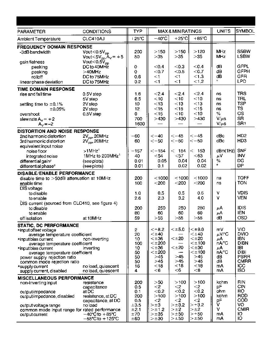
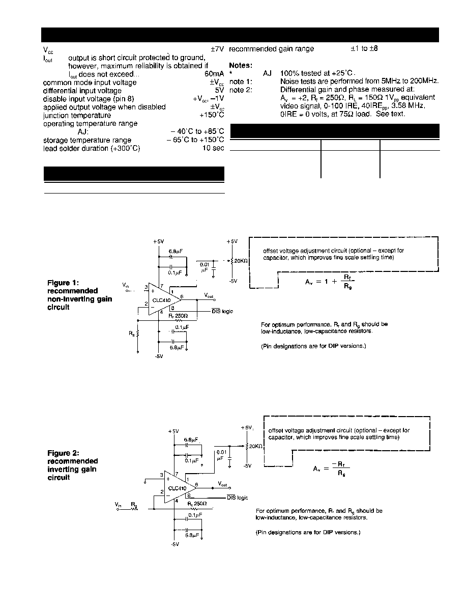
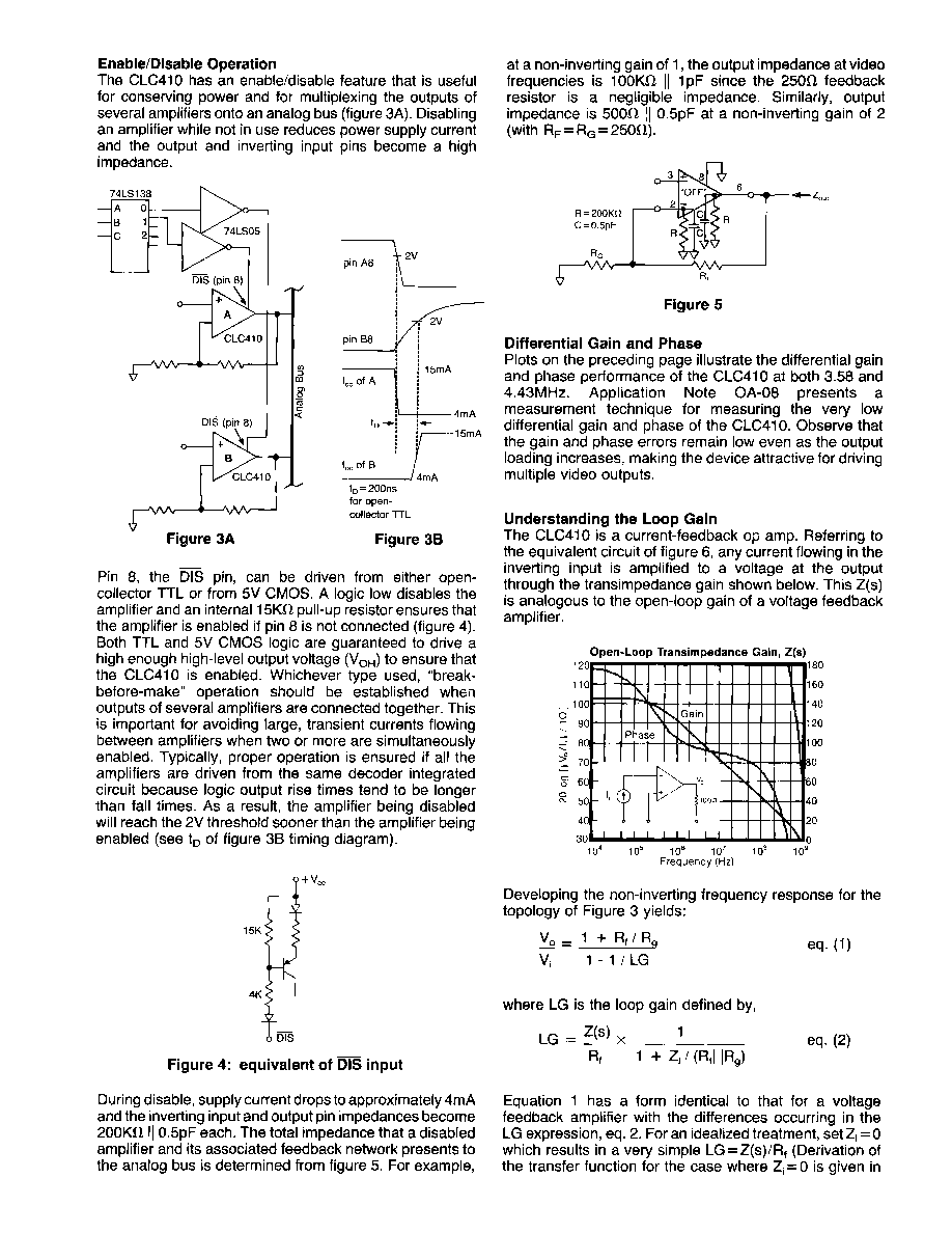
CLC410 Electrical Characteristics
(A
v
= +2, V
cc
= ±5V, R
L
= 100
, R
f
= 250
;
unless specified)
http://www.national.com
2
Min/max ratings are based on product characterization and simulation. Individual parameters are tested as noted. Outgoing quality levels are
determined from tested parameters.
CLC410 Typical Performance Characteristics
(T
A
= 25∞, A
v
= +2, V
CC
= ±5V, R
L
= 100
; unless specified)
Non-Inverting Frequency Response
Magnitude (1dB/div)
1
10
100
Phase (deg)
-90
-360
-180
-270
0
-450
V
out
= 0.5V
pp
A
v
= 2
R
f
= 249
A
v
= 1
R
f
= 402
A
v
= 10
R
f
= 200
A
v
= 5
R
f
= 200
Inverting Frequency Response
Magnitude (1dB/div)
1
10
100
Phase (deg)
-270
-540
-360
-450
-180
-630
V
out
= 0.5V
pp
A
v
= -2
R
f
= 249
A
v
= -1
R
f
= 301
A
v
= -10
R
f
= 200
A
v
= -5
R
f
= 200
Frequency (MHz)
Frequency (MHz)
http://www.national.com
4