 | –≠–ª–µ–∫—Ç—Ä–æ–Ω–Ω—ã–π –∫–æ–º–ø–æ–Ω–µ–Ω—Ç: CLC411 | –°–∫–∞—á–∞—Ç—å:  PDF PDF  ZIP ZIP |
N
CLC411
High-Speed Video Op Amp with Disable
General Description
The CLC411 combines a state-of-the-art complementary bipolar
process with National's patented current-feedback architecture to
provide a very high-speed op amp operating from ±15V supplies.
Drawing only 11mA quiescent current, the CLC411 provides a
200MHz small signal bandwidth and a 2300V/
µ
s slew rate while
delivering a continuous 70mA current output with ±4.5V output swing.
The CLC411's high-speed performance includes a 15ns settling time
to 0.1% (2V step) and a 2.3ns rise and fall time (6V step).
The CLC411 is designed to meet the requirements of professional
broadcast video systems including composite video and high definition
television. The CLC411 exceeds the HDTV standard for gain flatness
to 30MHz with it's ±0.05dB flat frequency response and exceeds
composite video standards with its very low differential gain and
phase errors of 0.02%, 0.03∞. The CLC411 is the op amp of choice
for all video systems requiring upward compatibility from NTSC and
PAL to HDTV.
The CLC411 features a very fast disable/enable (10ns/55ns) allowing
the multiplexing of high-speed signals onto an analog bus through the
common output connections of multiple CLC411's. Using the same
signal source to drive disable/enable pins is easy since "break-
before-make" is guaranteed.
The CLC411 is available in several versions:
CLC411AJP
-40∞C to +85∞C
8-pin plastic DIP
CLC411AJE
-40∞C to +85∞C
8-pin plastic SOIC
CLC411A8B
-55∞C to +125∞C
8-pin hermetic CERDIP,
MIL-STD-883
CLC411AMC
-55∞C to +125∞C
dice, MIL-STD-883, Level B
DESC SMD number: 5962-94566
June 1999
CLC411
High-Speed
Video Op Amp with Disab
le
Features
s
200MHz small signal bandwidth (1V
pp
)
s
±0.05dB gain flatness to 30MHz
s
0.02%, 0.03∞ differential gain, phase
s
2300V/
µ
s slew rate
s
10ns disable to high-impedance output
s
70mA continuous output current
s
±4.5V output swing into 100
load
s
±4.0V input voltage range
Applications
s
HDTV amplifier
s
Video line driver
s
High-speed analog bus driver
s
Video signal multiplexer
s
DAC output buffer
Pinout
DIP & SOIC
0.01
µ
F
0.1
µ
F
0.1
µ
F
6.8
µ
F
6.8
µ
F
0.01
µ
F
+V
r
-V
r
V
in
+
_
3
2
4
7
8
1
5
6
CLC411
25
R
T
R
g
Select R
T
to yield
R
in
= R
T
||R
g
R
f
V
out
DIS
-V
cc
+V
cc
Recommended
Inverting Gain
Configuration
0 Frequency (5MHz/div) 50
Magnitude (0.5dB/div)
Gain Flatness (A
v
=+2)
-
+
1
2
3
4
DIS
+V
cc
V
out
-V
r
+V
r
V
inv
V
non-inv
-V
cc
8
7
6
5
©
1999 National Semiconductor
Corporation
http://www.national.com
Printed in the U.S.A.

PARAMETERS
CONDITIONS
TYP
MIN/MAX RATINGS
UNITS
SYMBOL
Ambient Temperature
CLC411 AJ
+25
∞
C
-40
∞
C
+25
∞
C
+85
∞
C
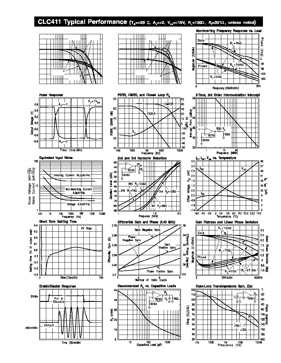
FREQUENCY DOMAIN RESPONSE
-3dB bandwidth
V
out
< 1V
pp
200
150
150
110
MHz
SSBW
V
out
< 6V
pp
75
50
50
40
MHz
LSBW
gain flatness
V
out
< 1V
pp
peaking
DC to 30MHz
0.05
0.2
0.2
0.3
dB
GFPL
rolloff
DC to 30MHz
0.05
0.2
0.2
0.4
dB
GFRL
peaking
DC to 200MHz
0.1
0.6
0.5
0.6
dB
GFPH
rolloff
DC to 60MHz
0.2
0.7
0.4
0.7
dB
GFRH
linear phase deviation
DC to 60MHz
0.3
1.0
1.0
1.0
∞
LPD
differential gain
4.43MHz, R
L
=150W
0.02
%
DG
differential phase
4.43MHz, R
L
=150W
0.03
∞
DP
TIME DOMAIN RESPONSE
rise and fall time
6V step
2.3
ns
TR
settling time to 0.1%
2V step
15
23
18
23
ns
TS
overshoot
2V step
5
15
10
15
%
OS
slew rate
6V step
2300
V/
µ
s
SR
DISTORTION AND NOISE RESPONSE (note 1)
2
ND
harmonic distortion
2V
pp
, 20MHz
-48
-35
-35
-35
dBc
HD2
3
RD
harmonic distortion
2V
pp
, 20MHz
-52
-42
-42
-35
dBc
HD3
equivalent noise input
voltage
>1MHz
2.5
nV/
Hz
VN
inverting current
>1MHz
12.9
pA/
Hz
ICI
non-inverting current
>1MHz
6.3
pA/
Hz
ICN
noise floor
>1MHz
-157
dBm
1Hz
SNF
integrated noise
1MHz to 200MHz
45
µ
V
INV
STATIC DC PERFORMANCE
*input offset voltage
±2
±13
±9.0
±14
mV
VIO
average temperature coefficient
+30
±50
____
±50
µ
V/∞C
DVIO
*input bias current
non-inverting
12
65
30
±20
µ
A
IBN
average temperature coefficient
±200
±400
____
±250
nA/∞C
DIBN
*input bias current
inverting
±12
±40
±30
±30
µ
A
IBI
average temperature coefficient
±50
±200
____
±150
nA/∞C
DIBI
power supply rejection ratio
56
48
50
48
dB
PSRR
common mode rejection ratio
52
44
46
44
dB
CMRR
*supply current
no load
11
14
12
12
mA
ICC
supply current
disabled
2.5
4.5
3.5
4.5
mA
ICCD
DISABLE/ENABLE PERFORMANCE (note 2)
disable time
to >50dB attenuation @10MHz
10
30
30
60
ns
TOFF
enable time
55
ns
TON
DIS voltage
pin 8
to disable
4.5
<3.0
<3.0
<3.0
V
VDIS
to enable
5.5
>7.0
>6.5
>6.5
V
VEN
off isolation
at 10MHz
59
55
55
55
dB
OSD
MISCELLANEOUS PERFORMANCE
non-inverting input resistance
1000
250
750
1000
k
RIN
non-inverting input capacitance
2.0
3.0
3.0
3.0
pF
CIN
output voltage range
no load
±6.0
±4.5
V
VO
output voltage range
R
L
=100
±4.5
±4.0
V
VOL
common mode input range
±4.0
±3.5
V
CMIR
output current
70
30
50
40
mA
IO
Min/max ratings are based on product characterization and simulation. Individual parameters are tested as noted. Outgoing quality levels
are determined from tested parameters.
CLC411 Electrical Characteristics
(A
(A
(A
(A
(A
V
V
V
V
V
= +2; V
= +2; V
= +2; V
= +2; V
= +2; V
CC
CC
CC
CC
CC
=
=
=
=
=
±±
±±
±
15V; R
15V; R
15V; R
15V; R
15V; R
L
L
L
L
L
= 100
= 100
= 100
= 100
= 100
; R
; R
; R
; R
; R
f
f
f
f
f
= 301
= 301
= 301
= 301
= 301
, unless noted)
, unless noted)
, unless noted)
, unless noted)
, unless noted)
Absolute Maximum Ratings
Miscellaneous Ratings
V
cc
±18V
I
out
125mA
common-mode input voltage
±V
cc
differential input voltage
±15V
maximum junction temperature
+150
∞
C
operating temperature range: AJ
-40∞C to +85∞C
storage temperature range
-65∞C to +150∞C
lead temperature (soldering 10 sec)
+300∞C
ESD (human body model)
1000V
Recommended gain range
±1 to ±10V/V
Notes: * AJ : 100% tested at +25∞C.
note 1
: Specifications guaranteed using 0.01mF bypass capacitors
on pins 1 & 5.
note 2
: Break before make is guaranteed.
http://www.national.com
2
Package Thermal Resistance
Package
JC
JA
AJP
65∞C/W
120∞C/W
AJE
55∞C/W
135∞C/W
A8B
25∞C/W
115∞C/W
Reliability Information
Transistor count
70
Inverting Frequency Response
Magnitude (1dB/div)
Frequency (MHz)
1
10
100
Phase (deg)
-270
-540
-360
-450
-180
-630
V
out
= 1V
pp
A
v
= -2
R
f
= 301
A
v
= -1
R
f
= 301
A
v
= -10
R
f
= 200
A
v
= -5
R
f
= 249
Non-Inverting Frequency Response
Magnitude (1dB/div)
Frequency (MHz)
1
10
100
Phase (deg)
-90
-360
-180
-270
0
-450
V
out
= 1V
pp
A
v
= 2
R
f
= 301
A
v
= 1
R
f
= 402
A
v
= 10
R
f
= 200
A
v
= 5
R
f
= 200
Frequency (MHz)
Frequency (MHz)
o
3
http://www.national.com
Description
The CLC411 is a high-speed current-feedback operational
amplifier which operates from ±15V power supplies.
The external supplies (±V
CC
) are regulated to lower
voltages internally. The amplifier itself sees
approximately ±6.5V rails. Thus the device yields
performance comparable to Comlinear's ±5V devices,
but with higher supply voltages. There is no degradation
in rated specifications when the CLC411 is operated
from ±12V. A slight reduction in bandwidth will be
observed with ±10V supplies. Operation at less than
±10V is not recommended.
A block diagram of the amplifier and regulator topology
is shown in Figure 2, "CLC411 Equivalent Circuit." The
regulators derive their reference voltage from an internal
floating zener voltage source. External control of the
zener reference pins can be used to level-shift amplifier
operation which is discussed in detail in the section
entitled "Extending Input/Output Range with V
r
."
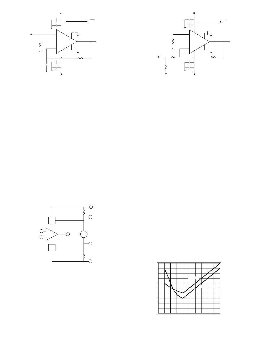
Power Supply Decoupling
There are four pins associated with the power supplies.
The V
CC
pins (4,7) are the external supply voltages. The
V
r
pins (5,1) are connected to internal reference nodes.
Figures 1 and 3 , "Recommended Non-inverting Gain
Circuit" and "Recommended Inverting Gain Circuit"
show the recommended supply decoupling scheme
with four ceramic and two electrolytic capacitors. The
ceramic capacitors must be placed immediately adjacent
to the device pins and connected directly to a good
0.01
µ
F
0.1
µ
F
0.1
µ
F
6.8
µ
F
6.8
µ
F
0.01
µ
F
+V
r
-V
r
V
in
+
_
3
2
4
7
8
1
5
6
CLC411
R
in
R
g
R
f
V
out
DIS
+V
cc
-V
cc
0.01
µ
F
0.1
µ
F
0.1
µ
F
6.8
µ
F
6.8
µ
F
0.01
µ
F
+V
r
-V
r
V
in
+
_
3
2
4
7
8
1
5
6
CLC411
25
R
T
R
g
Select R
T
to yield
R
in
= R
T
||R
g
R
f
V
out
DIS
-V
cc
+V
cc
Figure 3: Recommended
Inverting Gain Circuit
Figure 1: Recommended
Non-inverting Gain Circuit
low-inductance ground plane. Bypassing the V
r
pins will
reduce high frequency noise (>10MHz) in the amplifier.
If this noise is not a concern these capacitors may be
eliminated.
Differential Gain and Phase
The differential gain and phase errors of the CLC411
driving one doubly-terminated video load (R
L
=150
) are
s p e c i f i e d a n d g u a r a n t e e d i n t h e " E l e c t r i c a l
Characteristics" table. The "Typical Performance" plot,
"Differential Gain and Phase (4.43MHz)" shows the
differential gain and phase performance of the CLC411
when driving from one to four video loads. Application
note OA-08, "Differential Gain and Phase for Composite
Video Systems," describes in detail the techniques
used to measure differential gain and phase.
Feedback Resistor
The loop gain and frequency response for a current-
feedback operational amplifier is determined largely by
the feedback resistor, R
f
. The electrical characteristics
and typical performance plots contained within the
datasheet, unless otherwise stated, specify an R
f
of
301
, a gain of +2V/V and operation with ±15V power
supplies. The frequency response at different gain
settings and supply voltages can be optimized by
selecting a different value of R
f
. Generally, lowering R
f
will peak the frequency response and extend the
bandwidth while increasing its value will roll off the
response. For unity-gain voltage follower circuits, a
Figure 4: Recommended R
f
vs. Gain
Figure 2: CLC411 Equivalent Circuit
17k
1
7
5
4
3
2
6
17k
+V
cc
+V
r
V
z
-V
r
-V
cc
+
-
+
-
+
reg
_
reg
http://www.national.com
4
R
f
(
)
Gain (V/V)
500
400
300
200
100
0
0
1
2
3
4
5
6
7
8
9
10
Non-Inverting
Inverting
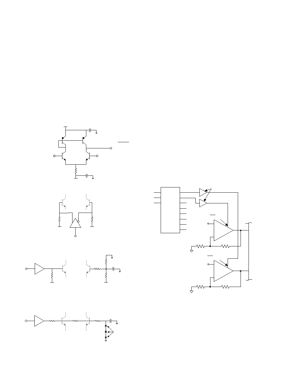
Figure 5C: ECL Interface
Figure 5B: Differential ECL Interface
Figure 5A: Disable Interface
Q3
+15V
-15V
3.57k
Q1
Q4
Q2
Disable
CLC411 pin 8, DISABLE
V
th
330
-5.2V
ECL
Gate
-5.2V
330
Q1
Q2
Q1,Q2 MPSH10
Q3,Q4 MPSH81
0.1
µ
F
0.1
µ
F
0.1
µ
F
-15V
-5.2V
10k
330
931
Q1
ECL
Gate
Q2
0.1
µ
F
1N914
332
TTL
Gate
50
50
50
Q1
Q2
non-zero R
f
must be used with current-feedback
operational amplifiers such as the CLC411. Application
note OA-13, "Current-Feedback Loop-Gain Analysis
and Performance Enhancements," explains the
ramifications of R
f
and how to use it to tailor the desired
frequency response with respect to gain. The equations
found in the application note should be considered as a
starting point for the selection of R
f
. The equations do
not factor in the effects of parasitic capacitance found
on the inverting input, the output nor across the feedback
resistor. Equations in OA-13 require values for R
f
(301
), Av (+2) and R
i
(inverting input resistance, 50
).
Combining these values yields a Z
t
* (optimum feedback
t r a n s i m p e d a n c e ) o f 4 0 0
. F i g u r e 4 e n t i t l e d
"Recommended R
f
vs. Gain" will enable the selection of
the feedback resistor that provides a maximally flat
frequency response for the CLC411 over its gain range.
The linear portion of the two curves (i.e. A
V
>4) results
from the limitation on R
g
(i.e. R
g
50
).
Enable/Disable Operation
The disable feature allows the outputs of several CLC411
devices to be connected onto a common analog bus
forming a high-speed analog multiplexer. When disabled,
the output and inverting inputs of the CLC411 become
high impedances. The disable pin has an internal pull-
up resistor which is pulled-up to an internal voltage, not
to the external supply. The CLC411 is enabled when pin
8 is left open or pulled-up to
+
7V and disabled when
grounded or pulled below
+
3V. CMOS logic devices are
necessary to drive the disable pin. For example, CMOS
logic with V
DD
+
7V will guarantee proper operation over
temperature. TTL voltage levels are inadequate for
controlling the disable feature.
For faster enable/disable operation than 15V CMOS
logic devices will allow, the circuit of Figure 5 is
recommended. A fast four-transistor comparator, Figure
5A, interfaces between the CLC411 DISABLE pin and
several standard logic families. This circuit has a
differential input between the bases of Q1 and Q2. As
such it may be driven directly from differential ECL
logic, as in shown in Figure 5B. Single-ended logic
families may also be used by establishing an appropriate
threshold voltage on the V
th
input, the base of Q2.
Figures 5C and 5D illustrate a single-ended ECL and
TTL interface respectively. The Disable input, the base
of Q1, is driven above and below the threshold, V
th
.
Fastest switching speeds result when the differential
voltage between the bases of Q1 and Q2 is kept to less
A
B
C
0
1
2
3
4
5
6
7
+
A
CLC411
CLC411
DIS (pin 8)
Buffers
DIS (pin 8)
-
+
B
-
Analog
Bus
Figure 6: General Multiplexing Circuit
5
http://www.national.com
Figure 5D: TTL Interface