CLC412
Dual Wideband Video Op Amp
General Description
The CLC412 combines a high speed complementary bipolar
process with National's current feedback topology to pro-
duce a very high speed dual op amp. The CLC412 provides
a 250MHz small signal bandwidth at a gain of +2V/V and a
1300V/µs slew rate while consuming only 50mW per ampli-
fier from
±
5V supplies.
The CLC412 offers exceptional video performance with its
0.02% and 0.02∞ differential gain and phase errors for NTSC
and PAL video signals while driving one back terminated
75
load. The CLC412 also offers a flat gain response of
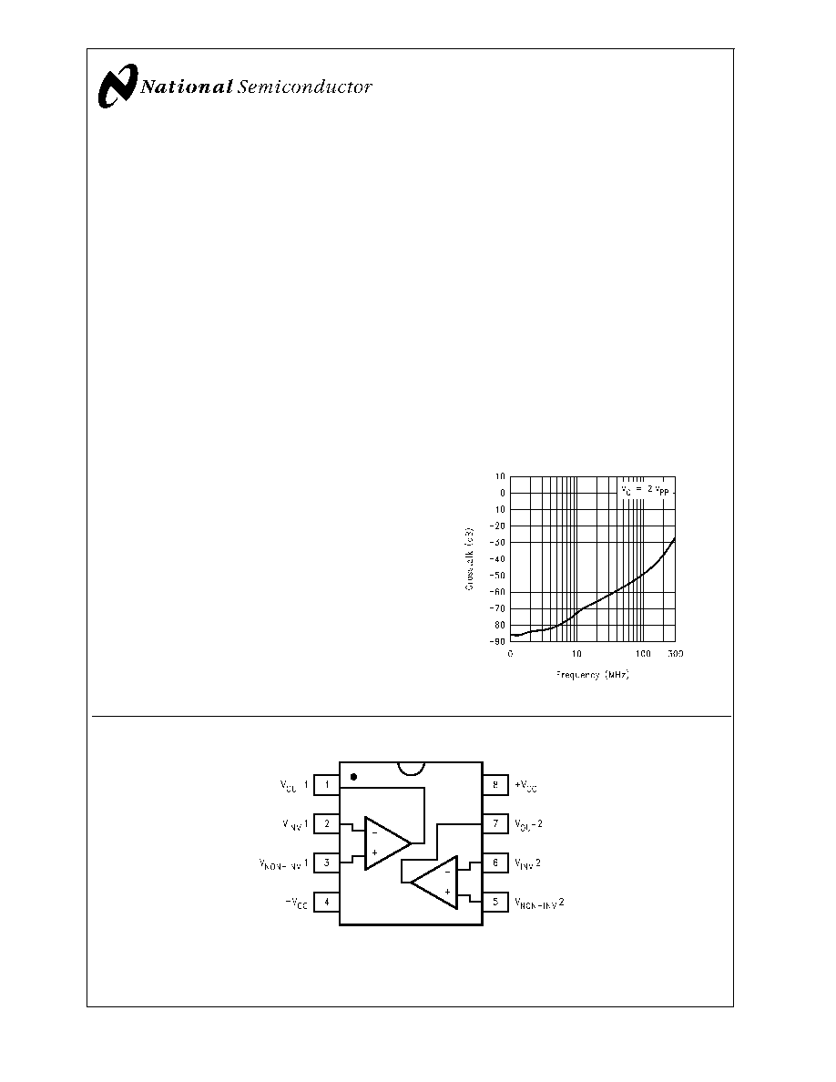
0.1dB to 30MHz and very low channel-to-channel crosstalk
of -76dB at 10MHz. Additionally, each amplifier can deliver a
70mA continuous output current. This level of performance
makes the CLC412 an ideal dual op amp for high density
broadcast quality video systems.
The CLC412's two very well matched amplifiers support a
number of applications such as differential line drivers and
receivers. In addition, the CLC412 is well suited for Sallen
Key active filters in applications such as anti-aliasing filters
for high speed A/D converters. Its small 8-pin SOIC package,
low power requirement, low noise and distortion allow the
CLC412 to serve portable RF applications such as IQ chan-
nels.
Enhanced Solutions (Military/Aerospace)
SMD Number: 5962-94719
Space level versions also available.
For more information, visit http://www.national.com/mil
Features
n
Wide bandwidth: 330MHz (A
V
= +1); 250MHz (A
V
= +2)
n
0.1dB gain flatness to 30MHz
n
Low power: 5mA/channel
n
Very low diff. gain, phase: 0.02%, 0.02∞
n
-76dB channel-to-channel crosstalk (10MHz)
n
Fast slew rate: 1300V/µs
n
Unity gain stable
Applications
n
HDTV, NTSC & PAL video systems
n
Video switching and distribution
n
IQ amplifiers
n
Wideband active filters
n
Cable drivers
n
DC coupled single-to-differential conversions
Channel-to-Channel Crosstalk
01272101
Connection Diagram
01272104
Pinout
DIP & SOIC
November 2001
CLC412
Dual
W
ideband
V
ideo
Op
Amp
© 2001 National Semiconductor Corporation
DS012721
www.national.com

Typical Application
01272103
01272102
Sallen-Key Low-Pass Filter
Ordering Information
Package
Temperature Range
Industrial
Part Number
Package Marking
NSC Drawing
8-pin plastic DIP
-40∞C to +85∞C
CLC412AJP
CLC412AJP
N08E
8-pin plastic SOIC
-40∞C to +85∞C
CLC412AJE
CLC412AJE
M08A
CLC412
www.national.com
2

Absolute Maximum Ratings
(Note 1)
If Military/Aerospace specified devices are required,
please contact the National Semiconductor Sales Office/
Distributors for availability and specifications.
V
CC
±
7V
I
OUT
Short Circuit protected to ground,
however maximum reliability is
obtained if I
OUT
does not exceed..
125mA
Common-Mode Input Voltage
±
V
CC
Maximum Junction Temperature
+150∞C
Operating Temperature Range
-40∞C to +85∞C
Storage Temperature Range
-65∞C to +150∞C
Lead Temperature (Soldering 10
sec)
+300∞C
ESD (Human Body Model)
1000V
Operating Ratings
Thermal Resistance
Package
(
JC
)
(
JA
)
MDIP
70∞C/W
125∞C/W
SOIC
65∞C/W
145∞C/W
Electrical Characteristics
(A
V
= +2, R
f
= 634
, V
CC
=
±
5 V, R
L
= 100
; Unless Specified).
Symbol
Parameter
Conditions
Typ
Min/Max Ratings
(Note 2)
Units
Ambient Temperature
CLC412AJ
+25∞C
-40∞C
+25∞C
+85∞C
Frequency Domain Response
SSBW
-3dB Bandwidth
V
OUT
<
0.5V
PP
250
150
175
135
MHz
LSBW
V
OUT
<
4.0V
PP
105
80
80
65
MHz
Gain Flatness
V
OUT
<
0.5V
PP
GFP
Peaking
DC to 30MHz
0.1
0.1
0.1
0.2
dB
GFR
Rolloff
DC to 30MHz
0.1
0.4
0.3
0.3
dB
LPD
Linear Phase Deviation
DC to 75MHz
0.5
1.3
1.0
1.0
deg
DG
Differential Gain
R
L
= 150
, 4.43MHz
0.02
0.04
0.04
0.08
%
DP
Differential Phase
R
L
= 150
, 4.43MHz
0.02
0.04
0.04
0.08
deg
Time Domain Response
TRS
Rise and Fall Time
0.5V Step
1.4
2.3
2.0
2.6
ns
TRL
4V Step
3.2
4.4
4.4
4.8
ns
TSS
Settling Time to 0.05%
2V Step
12
18
18
20
ns
OS
Overshoot
0.5V Step
8
15
15
15
%
SR
Slew Rate
2V Step
1300
1000
1000
800
V/µs
Distortion And Noise Response
HD2
2nd Harmonic Distortion
2V
PP
, 20MHz
-46
-42
-42
-38
dBc
HD3
3rd Harmonic Distortion
2V
PP
, 20MHz
-50
-46
-46
-42
dBc
IMD
3rd Order Intermodulation
Intercept
10MHz
43
≠
≠
≠
dBm
1Hz
Equivalent Input Noise
VN
Non-Inverting Voltage
>
1MHz
3.0
3.4
3.4
3.8
nV/
NICN
Inverting Current
>
1MHz
12.0
13.9
13.9
15.5
pA/
ICN
Non-Inverting Current
>
1MHz
2.0
2.6
2.6
3.0
pA/
SNF
Noise Floor
>
1MHz
-157
-156
-156
-155
dBm
1Hz
XTLKA
Crosstalk Input Referred
10MHz
-76
-70
-70
-70
dB
Static, DC Performance
VIO
Output Offset Voltage (Note 3)
±
2
±
10
±
6
±
12
mV
DVIO
Average Drift
±
30
±
60
-
±
60
µV/∞C
IBN
Input Bias Current (Note 3)
Non-Inverting
±
5
±
28
±
12
±
12
µA
DIBN
Average Drift
±
30
±
187
-
±
90
nA/∞C
IBI
Input Bias Current (Note 3)
Inverting
±
3
±
34
±
15
±
20
µA
DIBI
Average Drift
±
20
±
125
-
±
80
nA/∞C
CLC412
www.national.com
3
Electrical Characteristics
(Continued)
(A
V
= +2, R
f
= 634
, V
CC
=
±
5 V, R
L
= 100
; Unless Specified).
Symbol
Parameter
Conditions
Typ
Min/Max Ratings
(Note 2)
Units
PSRR
Power Supply Rejection Ratio
DC
50
46
46
44
dB
CMRR
Common Mode Rejection Ratio
DC
50
45
45
43
dB
ICC
Supply Current (Note 3)
R
L
=
10.2
13.6
12.8
12.8
mA
Miscellaneous Performance
RIN
Input Resistance
Non-Inverting
1000
300
500
500
k
CIN
Input Capacitance
Non-Inverting
1.0
2.0
2.0
2.0
pF
ROUT
Output Resistance
Closed Loop
0.04
0.6
0.3
0.2
VO
Output Voltage Range
R
L
=
+3.8, -3.3 +3.6, -2.9 +3.7, -3.0 +3.7, -3.0
V
VOL
R
L
= 100
+3.1, -2.9 +2.0, -2.5
±
2.7
±
2.7
V
VOLC
R
L
= 100
(0∞ to 70∞C)
+2.5, -2.6
V
CMIR
Input Voltage Range
Common Mode
±
2.2
±
1.4
±
2.0
±
2.0
V
IO
Output Current
70
25
45
45
mA
Note 1: "Absolute Maximum Ratings" are those values beyond which the safety of the device cannot be guaranteed. They are not meant to imply that the devices
should be operated at these limits. The table of "Electrical Characteristics" specifies conditions of device operation.
Note 2: Min/max ratings are based on product characterization and simulation. Individual parameters are tested as noted. Outgoing quality levels are determined
from tested parameters.
Note 3: AJ-level: spec. is 100% tested at +25∞C.
Typical Performance Characteristics
(T
A
= 25∞C, V
CC
=
±
5V, A
V
=
±
2V/V, R
f
= 634
, R
L
= 100
,
Unless Specified).
Non-Inverting Frequency Response
Inverting Frequency Response
01272105
01272106
CLC412
www.national.com
4

Typical Performance Characteristics
(T
A
= 25∞C, V
CC
=
±
5V, A
V
=
±
2V/V, R
f
= 634
, R
L
= 100
,
Unless Specified). (Continued)
Frequency Response vs. V
OUT
Small Signal Channel Matching
01272107
01272108
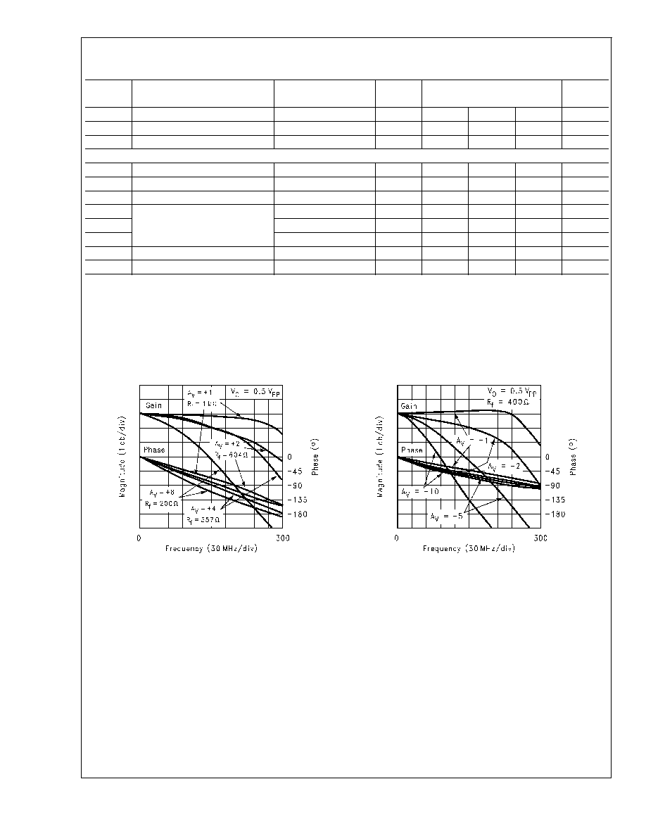
Gain Flatness for Various Gains
Frequency Response vs. Load (R
L
)
01272109
01272110
Pulse Response
Pulse Crosstalk
01272111
01272112
CLC412
www.national.com
5