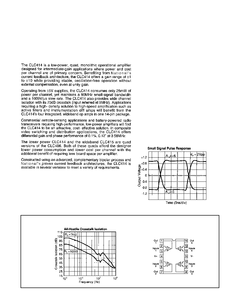
Features
s
90MHz small signal bandwidth
s
2mA quiescent current per amplifier
s
70dB channel isolation @ 5MHz
s
0.1%/0.12∞ differential gain/phase
s
16ns settling to 0.1%
s
100V/
µ
s slew rate
s
3.3ns rise and fall time (2V
pp
)
s
70mA output current
Applications
s
Composite video distribution amps
s
HDTV amplifiers
s
RGB-video amplifiers
s
CCD signal processing
s
Active filters
s
Instrumentation diff. amps
s
General purpose high density requirements
General Description
CLC414
Quad, Low-Power Monolithic Op Amp
N
June 1999
CLC414
Quad,
Lo
w-P
o
wer Monolithic Op Amp
Pinout
DIP & SOIC
© 1999 National Semiconductor Corporation
http://www.national.com
Printed in the U.S.A.
CLC414AJP
-40∞C to +85∞C
14-pin plastic DIP
CLC414AJE
-40∞C to +85∞C
14-pin plastic SOIC
CLC414ALC -40∞C to +85∞C
dice
CLC414A8B
-55∞C to +125∞C
14-pin hermetic CERDIP,
MIL-STD-883, Level B
DESC SMD number: 5962-91693
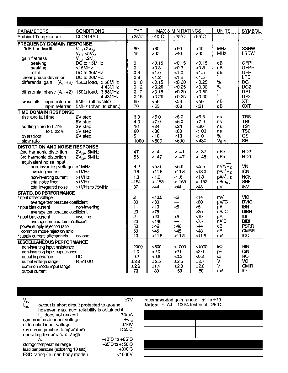
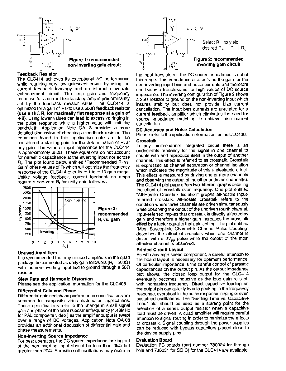
CLC414 Electrical Characteristics
(A
v
= +6, V
cc
= ±5V, R
L
= 100
, R
f
= 500
;
unless specified)
Absolute Maximum Ratings
Miscellaneous Ratings
http://www.national.com
2
Min/max ratings are based on product characterization and simulation. Individual parameters are tested as noted. Outgoing quality levels are
determined from tested parameters.
Package Thermal Resistance
Package
JC
JA
AJP
60∞C/W
110∞C/W
AJE
45∞C/W
115∞C/W
Reliability Information
Transistor count
152
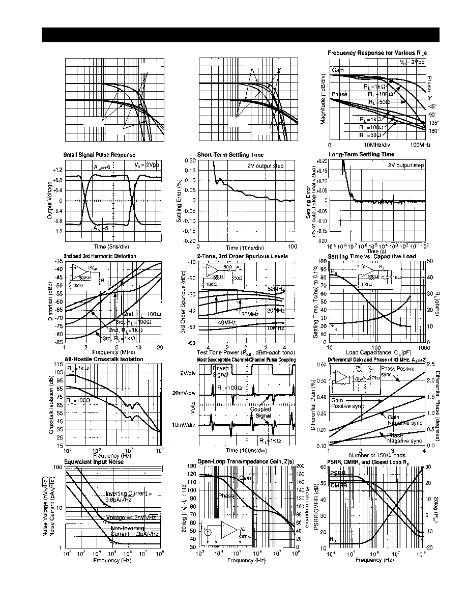
CLC414 Typical Performance Characteristics
(T
A
= 25∞, A
v
= +6, V
CC
= ±5V, R
L
= 100
, R
f
= 500
)
3
Non-Inverting Frequency Response
Magnitude (1dB/div)
1
10
100
Phase (deg)
-90
-360
-180
-270
0
-450
V
out
= 2V
pp
A
v
= 6
R
f
= 499
A
v
= 2
R
f
= 1.74k
A
v
= 10
R
f
= 200
Inverting Frequency Response
Magnitude (1dB/div)
1
10
100
Phase (deg)
-270
-540
-360
-450
-180
-630
V
out
= 2V
pp
A
v
= -2
R
f
= 1k
A
v
= -1
R
f
= 1k
A
v
= -10
R
f
= 499
A
v
= -6
R
f
= 499
Frequency (MHz)
Frequency (MHz)
3
http://www.national.com