Small Signal Pulse Response
5ns/div
Output Voltage
A =+6
v
V = 2Vpp
o
+1.2
+0.8
+0.4
0
-0.4
-0.8
-1.2
A =-5
v
Features
s
160MHz small signal bandwidth
s
5mA quiescent current per amplifier
s
70dB channel isolation @ 5MHz
s
0.03%/0.03∞ differential gain/phase
s
12ns settling to 0.1%
s
1500V/
µ
s slew rate
s
2.0ns rise and fall time (2V
pp
)
s
70mA output current per amplifier
Applications
s
Composite video distribution amps
s
HDTV amplifiers
s
RGB-video amplifiers
s
CCD signal processing
s
Active Filters
s
Instrumentation differential amps
s
Channelized EW
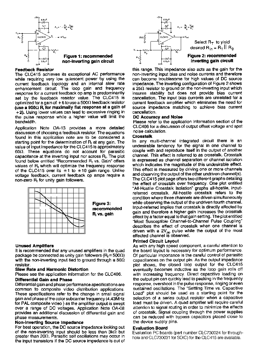
General Description
CLC415
Quad, Wideband Monolithic Op Amp
N
June 1999
CLC415
Quad,
Wideband Monolithic Op Amp
Non-Inverting Frequency Response
Magnitude (1dB/div)
1 Frequency (MHz) 100
Phase
0
-90
∞
-180
∞
-270
∞
-360
∞
-450
∞
V
o
= 2V
pp
A
v
= 6
R
f
= 499
A
v
= 2
R
f
= 698
A
v
= 10
R
f
= 200
Gain
Phase
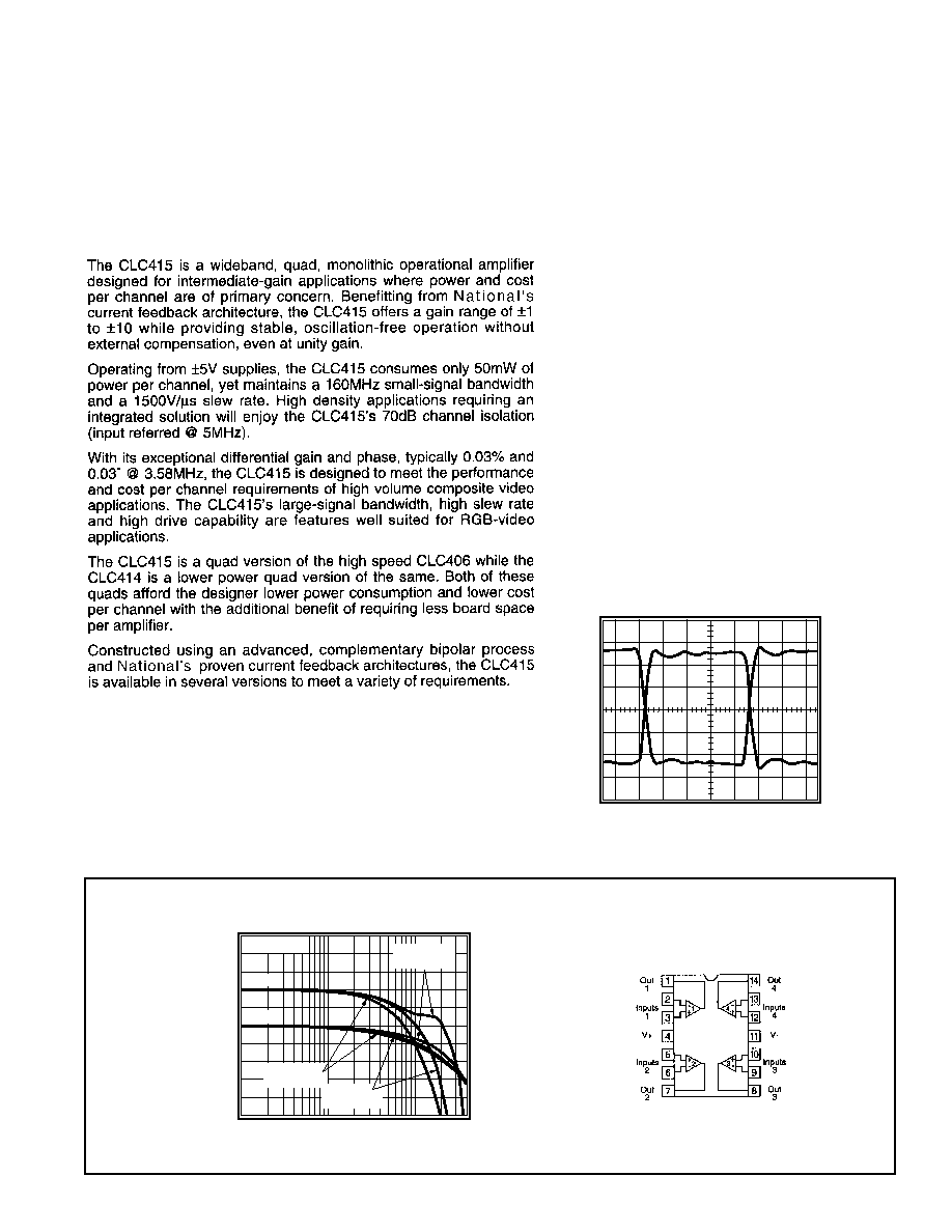
Pinout
DIP & SOIC
© 1999 National Semiconductor Corporation
http://www.national.com
Printed in the U.S.A.
CLC415AJP
-40∞C to +85∞C
14-pin plastic DIP
CLC415AJE
-40∞C to +85∞C
14-pin plastic SOIC
DESC SMD number: 5962-90994
CLC415 Electrical Characteristics
(A
v
= +6, V
cc
= ±5V, R
L
= 100
, R
f
= 500
;
unless specified)
2
Absolute Maximum Ratings
Miscellaneous Ratings
http://www.national.com
2
Min/max ratings are based on product characterization and simulation. Individual parameters are tested as noted. Outgoing quality levels are
determined from tested parameters.
Package Thermal Resistance
Package
JC
JA
AJP
55∞C/W
105∞C/W
AJE
45∞C/W
115∞C/W
CERDIP
30∞C/W
80∞C/W
Reliability Information
Transistor count
144
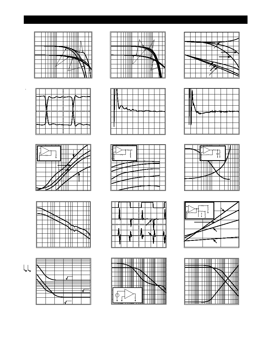
CLC415 Typical Performance Characteristics
(T
A
= 25∞, A
v
= +6,V
CC
= ±5V, R
L
= 100
,,
R
f
= 500
; unless specified)
Inverting Frequency Response
-180
∞
-270
∞
-360
∞
-450
∞
-540
∞
-630
∞
Phase
1 Frequency (MHz) 100
Magnitude (1dB/div)
Frequency Response for Various R s
Phase
0 20MHz/div 200MHz
V = 2Vpp
R
L
=50
=100
=100
=1k
=50
o
Magnitude (1dB/div)
L
0
∞
-45
∞
-90
∞
-135
∞
-180
∞
R
L
R
L
R
L
R
L
Small Signal Pulse Response
5ns/div
Output Voltage
A =+6
v
V = 2Vpp
o
+1.2
+0.8
+0.4
0
-0.4
-0.8
-1.2
A =-5
v
Short-Term Settling Time
0.20
0.15
0.10
0.05
0
-0.05
-0.10
-0.15
-0.20
Settling Error (%)
2V output step
Long-Term Settling Time
+0.20
+0.15
+0.10
+0.05
0
-0.05
-0.10
-0.15
-0.20
Settling Error
(% of output step final value)
2V output step
Time (s)
-40
-50
-60
-70
-80
Distortion (dBc)
1 2 5 10 20 50
Frequency (MHz)
2nd, R =100
L
3rd, R =100
L
3rd, R =1k
L
2nd, R =1k
L
100
L
R
-
+
2V
pp
500
2-Tone, 3rd Order Spurious Levels
-30
-40
-50
-60
-70
-80
3rd Order Spurious (dBc)
Test Tone Power (P , dBm-each tone)
-4 -2 0 2 4
-
+
50
out
P
100
500
50
40MHz
50MHz
30MHz
out
Settling Time vs. Capacitive Load
50
40
30
20
10
0
Settling Time, Ts(ns) to 0.05%
10 100 1000
Load Capacitance, C (pF)
50
40
30
20
10
0
R (ohms)
s
0.25
0.20
0.15
0.10
0.05
0
Differential Gain (%)
Number of 150 loads
1 2 3 4
Differential Phase (degrees)
.30
.25
.20
.15
.10
0
Phase Positive
sync
Equivalent Input Noise
100
Noise Voltage (nV/ Hz )
10 10 10 10 10 10 10
10
1
Frequency (Hz)
Noise Current (pA/ Hz )
2
3
4
6
7
8
5
Inverting Current =
11.5pA/ Hz
Voltage =3.0nV/ Hz
Gain
Phase
Gain
Phase
R
L
=1k
10 10 10 10 10 10 10 10 10 10
-9 -8 -7 -6 -5 -4 -3 -2 -1 0
R
s
PSRR, CMRR, and Closed Loop R
60
50
40
30
20
10
10 10 10 10 10
Frequency (Hz)
4
5
8
6
7
PSRR/CMRR (dB)
R
PSRR
Open-Loop Transimpedance Gain, Z(s)
130
120
110
100
90
80
70
60
50
40
30
10 10 10 10 10 10
Frequency (Hz)
4
5
3
6
7
200
180
160
140
120
100
80
60
40
20
20 log [ V /I / 1 ]
o
Phase (degrees)
o
CMRR
o
30
20
10
0
-10
-20
20log (R )
o
i
0 100
10ns/div
20MHz
10MHz
L
1k
R
s
-
+
100
500
C
L
T
s
105
95
85
75
65
55
45
35
25
15
10 10 10 10
Frequency (Hz)
5
8
6
7
Crosstalk Isolation (dB)
All Hostile Crosstalk Isolation
R =1k
L
R =100
L
Phase
Negative sync
Gain
Positive sync
Gain
Negative sync
V
out
-
+
75
75
75
V
out
Non-Inverting Current=
2.0pA/ Hz
50
20
5
2
Phase
Gain
2nd and 3rd Harmonic Distortion
Most Susceptible Channel-Channel Pulse Coupling
2V/div
20mV/div
Volts
Time (100ns/div)
10mV/div
Coupled
Signal
Driven
Signal
R =100
L
R =1k
L
8
-
+
100
V
o
I
i
Differential Gain and Phase (4.43 MHz, A =+2)
v
Non-Inverting Frequency Response
Magnitude (1dB/div)
1 Frequency (MHz) 100
Phase
0
-90
∞
-180
∞
-270
∞
-360
∞
-450
∞
V
o
= 2V
pp
A
v
= 6
R
f
= 499
A
v
= 2
R
f
= 698
A
v
= 10
R
f
= 200
Gain
Phase
V
o
= 2V
pp
A
v
= -2
R
f
= 698
A
v
= -1
R
f
= 802
A
v
= -10
R
f
= 402
A
v
= -6
R
f
= 499
3
http://www.national.com