 | –≠–ª–µ–∫—Ç—Ä–æ–Ω–Ω—ã–π –∫–æ–º–ø–æ–Ω–µ–Ω—Ç: CLC416 | –°–∫–∞—á–∞—Ç—å:  PDF PDF  ZIP ZIP |
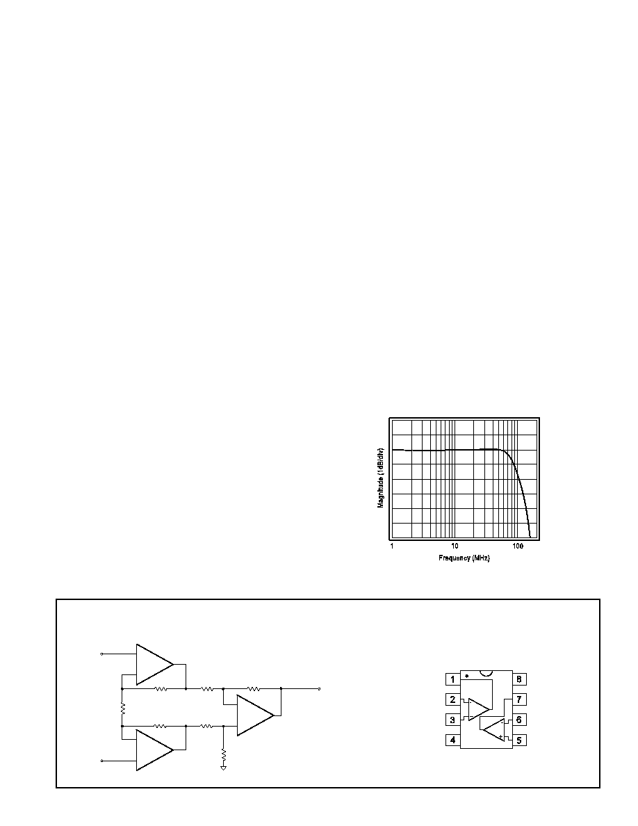
Typical Application Diagram
Instrumentation Amplifier
Pinout
DIP & SOIC
CLC416
Dual Low-Power, 120MHz Op Amp
September 1998
Features
s
0.01%, 0.03∞ D
G
, D
s
Very low input bias current: 100nA
s
High input impedance: 6M
s
120MHz -3dB bandwidth (A
v
= +2)
s
Low power
s
High output current: 60mA
s
Low-cost
Applications
s
Desktop video systems
s
Video distribution
s
Flash A/D driver
s
High-speed driver
s
High-source impedance applications
s
Professional video processing
s
High resolution monitors
General Description
The CLC416 is a dual, wideband (120MHz) op amp. The
CLC416 consumes only 39mW per channel and can source or
sink an output current of 60mA. These features make the
CLC416 a versatile, high-speed solution for demanding
applications that are sensitive to both power and cost.
Utilizing National's proven architectures, this dual current
feedback amplifier surpasses the performance of alternative
solutions and sets new standards for low power. This power-
conserving dual op amp achieves low distortion with -80dBc and
-80dBc second and third harmonics respectively. Many high
source impedance applications will benefit from the CLC416's
6M
input impedance. And finally, designers will have a bipolar
part with an exceptionally low 100nA non-inverting bias current.
With 0.1dB flatness to 30MHz and low differential gain and phase
errors, the CLC416 is an ideal part for professional video
processing and distribution. The 120MHz -3dB bandwidth (A
v
=
+2) coupled with a 400V/
µ
s slew rate also makes the CLC416
a perfect choice in cost-sensitive applications such as video
monitors, fax machines, copiers, and CATV systems.
V
o
1
V
inv
1
V
non-inv
1
-V
CC
V
o
2
V
inv
2
V
non-inv
2
+V
CC
+
-
348
1/2
CLC416
R
1
348
-
+
1/2
CLC416
348
348
V
out
= 3(V
2
- V
1
)
348
348
348
-
+
CLC405
V
1
V
2
Frequency Response (A
v
= +2V/V)
CLC416
Dual Low-Power
, 120MHz Op
Amp
N
© 1998 National Semiconductor Corporation
http://www.national.com
Printed in the U.S.A.

PARAMETERS
CONDITIONS
TYP
MIN/MAX RATINGS
UNITS
NOTES
Ambient Temperature
CLC416AJ
+25∞C
+25∞C
0 to 70∞C
-40 to 85∞C
FREQUENCY DOMAIN RESPONSE
-3dB bandwidth
V
out
< 1.0V
pp
120
65
45
45
MHz
V
out
< 5.0V
pp
52
40
36
35
MHz
1
±0.1dB bandwidth
V
out
< 1.0V
pp
30
15
MHz
gain flatness
V
out
< 1.0V
pp
peaking
DC to 200MHz
0.1
0.7
0.8
1.0
dB
rolloff
<30MHz
0
0.3
0.6
0.6
dB
linear phase deviation
<20MHz
0.3
0.6
0.7
0.7
deg
differential gain
4.43MHz, R
L
=150
0.01
0.04
0.04
0.04
%
differential phase
4.43MHz, R
L
=150
0.03
0.08
0.11
0.12
deg
TIME DOMAIN RESPONSE
rise and fall time
2V step
4.3
6.5
7.2
7.4
ns
settling time to 0.05%
2V step
22
30
38
41
ns
overshoot
2V step
3
12
12
12
%
slew rate
A
V
= +2
2V step
400
300
260
250
V/
µ
s
A
V
= -1
1V step
700
V/
µ
s
DISTORTION AND NOISE RESPONSE
2
nd
harmonic distortion
2V
pp
, 1MHz
-80
dBc
3
rd
harmonic distortion
2V
pp
, 1MHz
-80
dBc
2
nd
harmonic distortion
2V
pp
, 10MHz
-65
-55
-50
-47
dBc
3
rd
harmonic distortion
2V
pp
, 10MHz
-57
-50
-45
-45
dBc
equivalent input noise
voltage
>1MHz
5
6.3
6.6
6.7
nV/
Hz
inverting current
>1MHz
12
15
16
17
pA/
Hz
non-inverting current
>1MHz
3
3.8
4.0
4.2
pA/
Hz
crosstalk, input referred
2V
pp
, 10MHz
72
66
66
66
dB
STATIC DC PERFORMANCE
input offset voltage
1
5
7
8
mV
A
average drift
30
50
50
µ
V/∞C
input bias current
non-inverting
100
900
1600
2800
nA
A
average drift
3
8
11
nA/∞C
input bias current
inverting
1
5
6
8
µ
A
A
average drift
17
40
45
nA/∞C
power supply rejection ratio
DC
52
47
47
45
dB
common-mode rejection ratio
DC
50
45
45
43
dB
supply current per channel
R
L
=
3.9
4.5
4.6
4.9
mA
A
MISCELLANEOUS PERFORMANCE
input resistance
non-inverting
6
3
2.4
1
M
input capacitance
non-inverting
1
2
2
2
pF
common mode input range
±2.2
±1.8
±1.7
±1.5
V
output voltage range
R
L
= 100
+3.5,-2.9
+3.1/-2.8
+2.9/-2.7
+2.4/-1.7
V
output voltage range
R
L
=
+4.0,-3.4
+3.9/-3.3
+3.8/-3.2
+3.7/-2.8
V
output current
60
44
38
20
mA
output resistance, closed loop
0.06
0.2
0.25
0.4
Recommended gain range +1 to +40V/V
Transistor count = 110
Min/max ratings are based on product characterization and simulation. Individual parameters are tested as noted. Outgoing quality levels are
determined from tested parameters.
CLC416 Electrical Characteristics
(A
V
= +2, R
f
= 348
: V
cc
= + 5V, R
L
= 100
unless specified)
Absolute Maximum Ratings
supply voltage
±7V
I
out
is short circuit protected to ground
common-mode input voltage
±Vcc
maximum junction temperature
+175∞C
storage temperature range
-65∞C to +150∞C
lead temperature (soldering 10 sec)
+300∞C
ESD rating (human body model)
1000V
Notes
1) At temps < 0∞C, spec is guaranteed for R
L
= 500
.
A) J-level: spec is 100% tested at +25∞C.
Ordering Information
Model
Temperature Range
Description
CLC416AJP
-40
∞
C to +85
∞
C
8-pin PDIP
CLC416AJE
-40
∞
C to +85
∞
C
8-pin SOIC
Package Thermal Resistance
Package
JC
JA
Plastic (AJP)
80∞C/W
95∞C/W
Surface Mount (AJE)
95∞C/W
115∞C/W
http://www.national.com
2
CLC416 Typical Performance Characteristics
(V
cc
= ±5V, A
v
= +2, R
f
= 348
,,
R
L
= 100
; unless specified)
Frequency Response
Normalized Magnitude (1dB/div)
Frequency (MHz)
1
10
100
V
o
= 0.5V
pp
Phase (deg)
-90
-180
-450
-270
-360
0
A
v
= 1
R
f
= 1.65k
A
v
= 2
R
f
= 348
A
v
= 4
R
f
= 200
A
v
= 10
R
f
= 100
Inverting Frequency Response
Normalized Magnitude (1dB/div)
Frequency (MHz)
1
10
100
Phase (deg)
-270
-360
-630
-450
-540
-180
-90
0
A
v
= -1
R
f
= 2k
V
o
= 0.5V
pp
A
v
= -4
R
f
= 255
A
v
= -10
R
f
= 200
A
v
= -2
R
f
= 348
Frequency Response vs. R
L
Magnitude (1dB/div)
Frequency (MHz)
1
10
100
Phase (deg)
-90
-180
-450
-270
-360
0
R
L
= 100
V
o
= 1V
pp
A
v
= +2
R
L
= 1k
R
L
= 50
R
L
= 50
R
L
= 100
R
L
= 1k
Frequency Response vs. V
out
Magnitude (1dB/div)
Frequency (MHz)
1
10
100
1V
pp
A
v
= +2
0.2V
pp
2V
pp
5V
pp
Frequency Response vs. C
L
Magnitude (1dB/div)
Frequency (MHz)
1
10
100
V
o
= 1V
pp
R
s
= 107
C
L
= 10pF
R
s
= 39.25
C
L
= 47pF
R
s
= 27.4
C
L
= 100pF
R
s
= 8
C
L
= 1000pF
R
s
1k
348
348
C
L
Open Loop Transimpedance Gain, Z(s)
20 log [|V
o
/|
i
|] (dB
)
1k
10M
100M
Frequency (Hz)
130
110
90
70
50
30
Phase (deg)
200
160
120
80
40
0
Gain
Phase
1M
100k
10k
100
-
+
CLC416
V
o
I
i
Maximum Output Voltage vs. R
L
Maximum Output Voltage (V)
Load (
)
0
100
200
300
400
-4
-2
0
2
4
500
600
Recommended R
s
vs. Capacitive Load
R
s
(
)
C
L
(pF)
0
20
40
60
80
100
120
10
100
1000
2nd & 3rd Harmonic Distoration
Distortion Level (dBc)
Frequency (MHz)
1
10
-70
-80
-90
-60
-50
-40
V
o
= 2V
pp
3rd, R
L
= 100
2nd, R
L
= 100
2nd, R
L
= 1k
3rd, R
L
= 1k
2nd Harmonic Distortion vs. P
out
Distortion (dBc)
Output Power (dBm)
-90
-85
-80
-75
-70
-65
-60
-55
-10
-5
0
5
10
1MHz
500kHz
5MHz
10MHz
50
348
348
50
P
o
3rd Harmonic Distortion vs. P
out
Distortion (dBc)
Output Power (dBm)
-100
-90
-80
-70
-60
-50
-40
-10
-5
0
5
10
1MHz
500kHz
5MHz
10MHz
50
348
348
50
P
o
Differential Gain & Phase
Gain (%)
Number of 150
Loads
0
1
2
4
Phase (deg)
0
0.01
0.03
0.02
0.06
0.03
0.09
0.04
0.12
0.05
0.15
0.06
0.18
0.07
0.21
0.08
0.24
0.09
0.27
0.1
0.30
Phase Negative Sync
Phase Positive Sync
Gain Positive Sync
Gain Negative
Sync
3
Small Signal Pulse Response
Output Voltage (V)
Time (5ns/div)
-0.08
-0.06
-0.04
-0.02
0
0.02
0.04
0.06
0.08
A
v
= +1
A
v
= -1
Large Signal Pulse Response
Output Voltage (V)
Time (5ns/div)
-2
-1
0
1
2
A
v
= +2
A
v
= -2
PSRR and CMRR
PSRR/CMRR (dB)
10k
100k
1M
Frequency (Hz)
10M
100M
60
50
40
30
20
10
PSRR
CMRR
3
http://www.national.com
CLC416 Typical Performance Characteristics
(V
cc
= ±5V, A
v
= +2, R
f
= 348
,,
R
L
= 100
; unless specified)
CLC416 OPERATION
Description
The CLC416 is a dual current feedback amplifier with
the following features:
s
Differential gain and phase errors of 0.01%
and 0.03∞ into a 150
load
s
Low, 3.9mA, supply current per amplifier
The professional video quality differential gain and
phase errors and low power capabilities of the CLC416
make this product a good choice for video applications.
Gain
The non-inverting and inverting gain equations for the
CLC416 are as follows:
Non-inverting Gain:
Inverting Gain:
Where R
f
is the feedback resistor and R
g
is the gain
setting resistor. Figure 1 shows the general non-invert-
ing gain configuration including the recommended
bypass capacitors.
Figure 1: Recommended Non-Inverting Gain Circuit
Feedback Resistor Selection
The feedback resistor, R
f
, determines the loop gain
and frequency response of a current feedback
amplifier. Optimum performance of the CLC416, at a
gain of +2V/V, is achieved with R
f
equal to 348
. The
frequency response plots in the typical performance
section illustrate the recommended R
f
for several
gains. Within limits, R
f
can be adjusted to optimize the
frequency response.
s
Decrease R
f
to peak frequency response and
extend bandwidth
s
Increase R
f
to roll off frequency response and
reduce bandwidth
As a rule of thumb, if the recommended R
f
is doubled,
the bandwidth will be cut in half.
Channel Matching
Channel matching and crosstalk efficiency are largely
dependent on board layout. The layout of National's
dual amplifier evaluation boards are designed to produce
optimum channel matching and isolation. Typical
channel matching for the CLC416 is shown in Figure 2.
Figure 2: Channel Matching
The CLC416's channel-to-channel isolation is better
than 70dB for input frequencies of 4MHz. Input
referred crosstalk vs. frequency is illustrated in Figure 3.
Typical DC Errors vs. Temperature
Offset Voltage (mV)
Temperature (
∞
C)
6
5
4
1
-50
0
100
3
2
I
BN
Bias Current (
µ
A)
1
0
-1
-2
-3
50
I
BI
V
IO
Equivalent Input Noise
Noise Voltage (nV/
Hz)
Frequency (Hz)
100
10
1
1k
100
10k
100k
1M
10M
Noise Current (pA/
Hz)
100
10
1
Inverting Current = 12pA/
Hz
Voltage = 5nV/
Hz
Non-Inverting Current = 3pA/
Hz
Power Derating Curves
Power (W)
Ambient Temperature (
∞
C)
0.8
1.0
0.6
0
0
20
40
60
80
100
120 140
160 180
0.4
0.2
AJE
AJP
1
R
R
f
g
+
-
R
R
f
g
+
-
CLC416
R
f
0.1
µ
F
6.8
µ
F
V
o
V
in
+V
cc
0.1
µ
F
6.8
µ
F
-V
cc
R
L
R
g
R
in
g
Magnitude (0.5dB/div)
Frequency (MHz)
1
10
100
A
v
= +2
R
L
= 100
V
o
= 2V
pp
Phase (deg)
-450
-360
-270
-180
-90
0
Channel B
Channel B
Channel A
Channel A
http://www.national.com
4
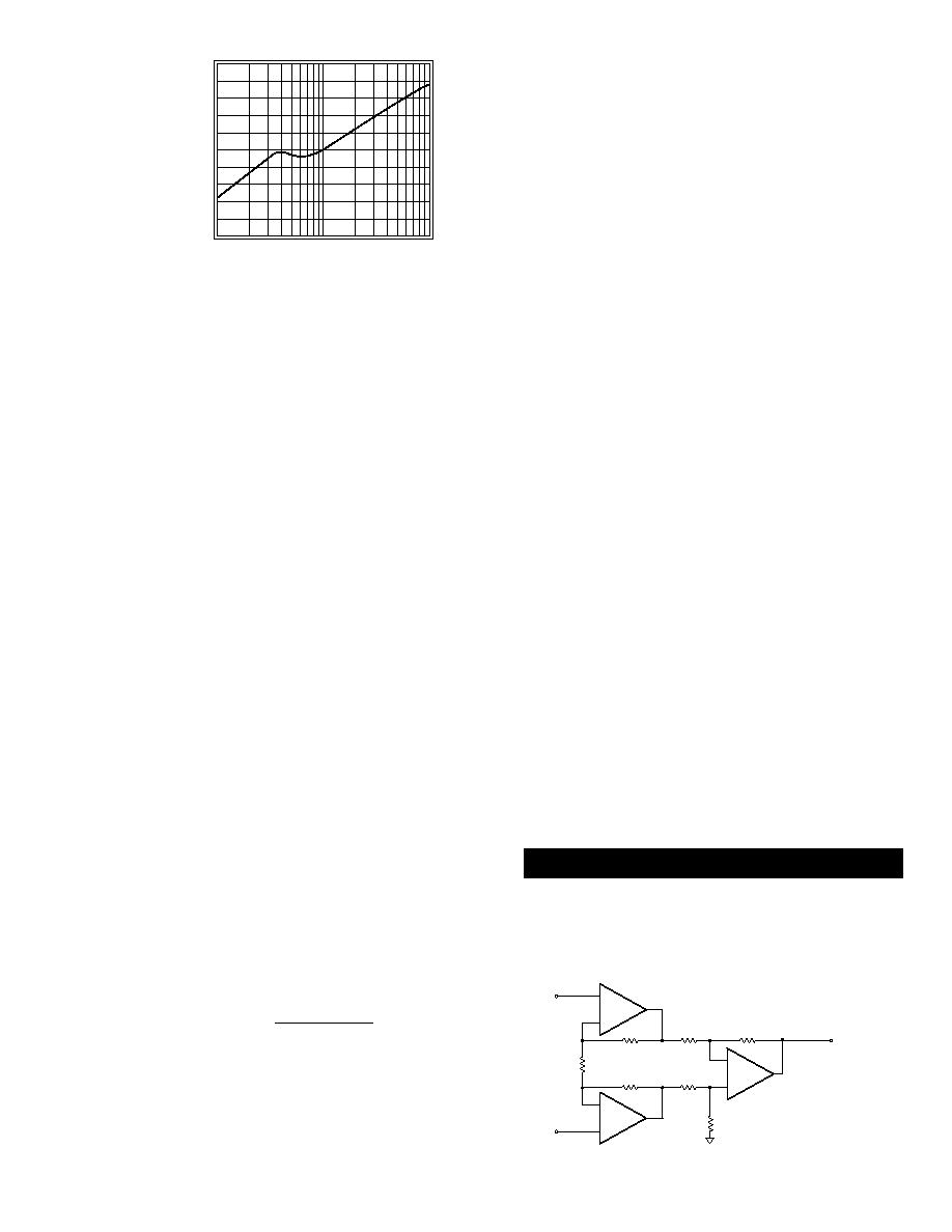
Figure 3: Input Referred Crosstalk vs. Frequency
Driving Cables and Capacitive Loads
When driving cables, double termination is used to
prevent reflections. For capacitive load applications, a
small series resistor at the output of the CLC416 will
improve stability. The
R
s
vs. Capacitive Load plot,
in the
Typical Performance section, gives the
recommended series resistance value for optimum
flatness at various capacitive loads.
Power Dissipation
The power dissipation of an amplifier can be described
in two conditions:
s
Quiescent Power Dissipation -
P
Q
(No Load Condition)
s
Total Power Dissipation -
P
T
(with Load Condition)
The following steps can be taken to determine the
power consumption for each CLC416 amplifier:
1. Determine the quiescent power
P
Q
= I
cc
(V
CC
- V
EE
)
2. Determine the RMS power at the output stage
P
O
= (V
cc
- V
load
) (I
load
), where V
load
and I
load
are the RMS voltage and current across the
external load.
3. Determine the total RMS power
P
T
= P
Q
+ P
O
Add the total RMS powers for both channels to deter-
mine the power dissipated by the dual.
The maximum power that the package can dissipate at
a given temperature is illustrated in the
Power
Derating curves in the Typical Performance section.
The power derating curve for any package can be
derived by utilizing the following equation:
where: T
amb
= Ambient temperature (∞C)
JA
= Thermal resistance, from junction to
ambient, for a given package (∞C/W)
Layout Considerations
A proper printed circuit layout is essential for achieving
high frequency performance. National provides
evaluation boards for the CLC416 (CLC730038 - DIP,
CLC730036 - SOIC) and suggests their use as a guide
for high frequency layout and as an aid for device test-
ing and characterization.
Supply bypassing is required for best performance.
The bypass capacitors provide a low impedance return
current path at the supply pins. They also provide high
frequency filtering on the power supply traces. Other
layout factors play a major role in high frequency
performance. The following are recommended as a
basis for high frequency layout:
1. Include 6.8
µ
F tantalum and 0.1
µ
F ceramic
capacitors on both supplies.
2. Place the 6.8
µ
F capacitors within 0.75 inches
of the power pins.
3. Place the 0.1
µ
F capacitors within 0.1 inches
of the power pins.
4. Remove the ground plane under and around
the part, especially near the input and output
pins to reduce parasitic capacitance.
5. Minimize all trace lengths to reduce series
inductances.
Additional information is included in the evaluation
board literature.
SPICE Models
SPICE models provide a means to evaluate amplifier
designs. Free SPICE models are available for
National's monolithic amplifiers that:
s
Support Berkeley SPICE 2G and its many
derivatives
s
Reproduce typical DC, AC, Transient, and
Noise performance
s
Support room temperature simulations
The
readme file that accompanies the diskette lists
released models, and provides a list of modeled para-
meters. The application note OA-18, Simulation
SPICE Models for National's Op Amps, contains
schematics and a reproduction of the
readme file.
Applications Circuits
Instrumentation Amplifier
An instrumentation circuit is shown on the front page
and reproduced in Figure 4. The DC CMRR can be
fine tuned by adjusting R
1
.
Figure 4: Instrumentation Amplifier
P
(175
Tamb)
JA
=
∞ -
+
-
348
1/2
CLC416
R
1
348
-
+
1/2
CLC416
348
348
V
out
= 3(V
2
- V
1
)
348
348
348
-
+
CLC405
V
1
V
2
Crosstalk (dB)
Frequency (MHz)
-120
-100
-80
-60
-40
-20
1
100
10
5
http://www.national.com