 | –≠–ª–µ–∫—Ç—Ä–æ–Ω–Ω—ã–π –∫–æ–º–ø–æ–Ω–µ–Ω—Ç: CLC417 | –°–∫–∞—á–∞—Ç—å:  PDF PDF  ZIP ZIP |
Features
s
0.01%, 0.03∞ D
G
, D
s
High output current: 60mA
s
High input impedance: 6M
s
Gains of +1, +2 with no external
components
s
Low power
s
Very low input bias currents: 100nA
s
Excellent gain accuracy: 0.1%
s
High speed: 120MHz -3dB BW
s
Low-cost
Applications
s
Desktop video systems
s
Video distribution
s
Flash A/D driver
s
High-speed line driver
s
High-source impedance applications
s
Professional video processing
s
High resolution monitors
General Description
The CLC417 is a dual, low-cost, high-speed (120MHz) buffer which
features user-programmable gains of +2, +1, and -1V/V. The
CLC417's high 60mA output current, coupled with its ultra-low
39mW per channel power consumption makes it the ideal choice for
demanding applications that are sensitive to both power and cost.
Utilizing National's proven architectures, this dual current feedback
amplifier surpasses the performance of alternate solutions with a
closed-loop design that produces new standards for buffers in gain
accuracy, input impedance, and input bias currents. The CLC417's
internal feedback network provides an excellent gain accuracy of
0.1%. High source impedance applications will benefit from the
CLC417's 6M
input impedance along with its exceptionally low
100nA input bias current.
With exceptional gain flatness and low differential gain and phase
errors, the CLC417 is very useful for professional video processing
and distribution. A 120MHz -3dB bandwidth coupled with a 400V/
µ
s
slew rate also make the CLC417 a perfect choice in cost-sensitive
applications such as video monitors, fax machines, copiers, and
CATV systems. Back-terminated video applications will be
enhanced by a gain of +2 configuration which requires no external
gain components reducing costs and board space.
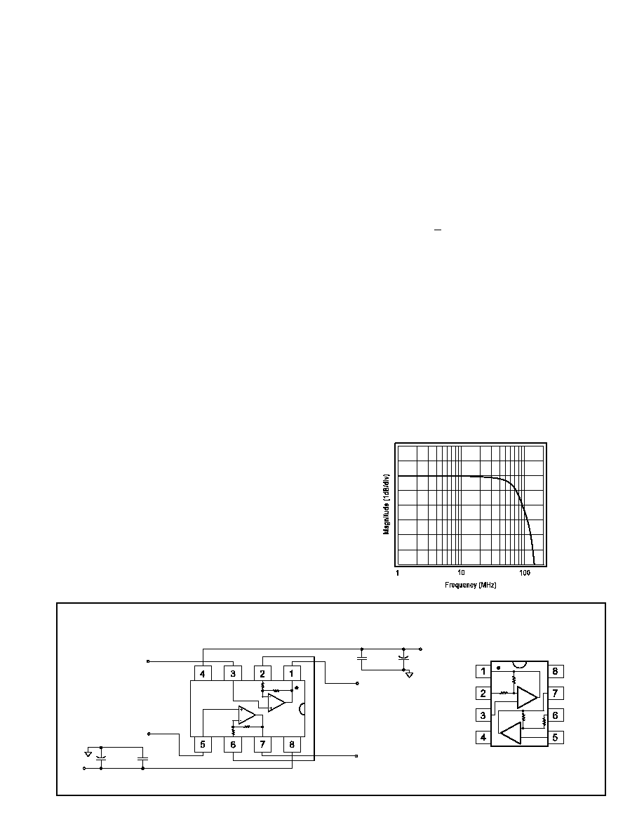
Frequency Response (A
V
= +2V/V)
Pinout
DIP & SOIC
-5V
0.1
µ
F
6.8
µ
F
+5V
0.1
µ
F
6.8
µ
F
V
out
2
V
in
1
CLC417
V
in
2
V
out
1
250
250
250
250
V
out
1 ≠ V
out
2 = (V
in
1 ≠ V
in
2) x 2
Typical Application
Differential Input/Differential Output Amplifier
CLC417
Dual Low-Power, Programmable Gain Buffer
September 1998
CLC417
Dual Low-Power
, Programmable Gain Buffer
OUT1
-IN1
+IN1
-V
CC
OUT2
-IN2
+IN2
+V
CC
250
+
-
+
-
250
250
250
N
© 1998 National Semiconductor Corporation
http://www.national.com
Printed in the U.S.A.
http://www.national.com
2
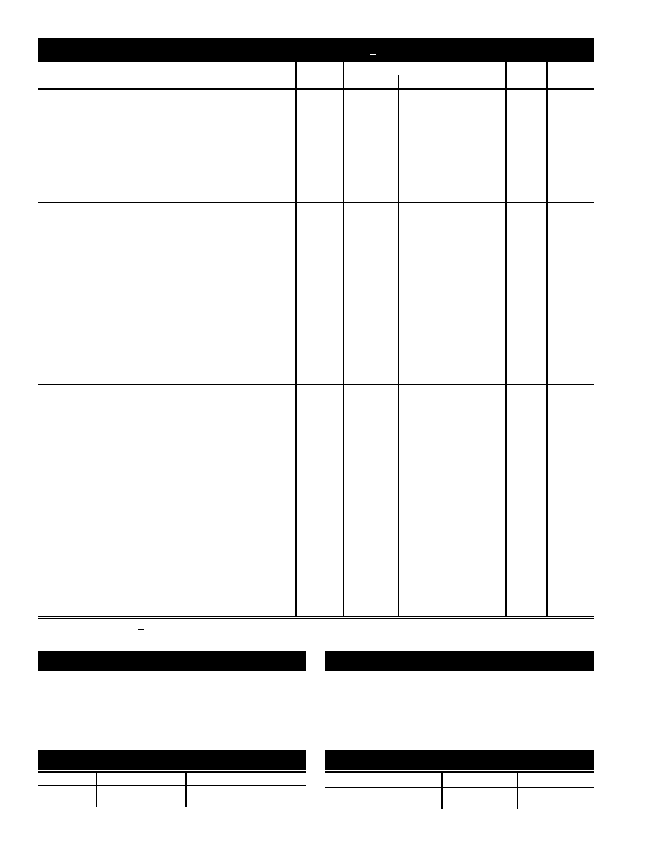
PARAMETERS
CONDITIONS
TYP
MIN/MAX RATINGS
UNITS
NOTES
Ambient Temperature
CLC417AJ
+25∞C
+25∞C
0 to 70∞C
-40 to 85∞C
FREQUENCY DOMAIN RESPONSE
-3dB bandwidth
V
out
< 1.0V
pp
120
85
65
60
MHz
V
out
< 5.0V
pp
52
40
36
35
MHz
1
±0.1dB bandwidth
V
out
< 1.0V
pp
50
15
MHz
gain flatness
V
out
< 1.0V
pp
peaking
DC to 200MHz
0
0.5
0.6
0.8
dB
rolloff
<30MHz
0.05
0.5
0.65
0.7
dB
linear phase deviation
<20MHz
0.3
0.6
0.7
0.7
deg
differential gain
4.43MHz, RL=150
0.01
0.04
0.04
0.04
%
differential phase
4.43MHz, RL=150
0.03
0.08
0.11
0.12
deg
TIME DOMAIN RESPONSE
rise and fall time
2V step
4.3
6.5
7.2
7.4
ns
settling time to 0.05%
2V step
22
30
38
41
ns
overshoot
2V step
3
12
12
12
%
slew rate
A
v
= +2
2V step
400
300
260
250
V/
µ
s
A
v
= -1
1V step
700
V/
µ
s
DISTORTION AND NOISE RESPONSE
2nd harmonic distortion
2V
pp
, 1MHz
-80
dBc
3rd harmonic distortion
2V
pp
, 1MHz
-80
dBc
2nd harmonic distortion
2V
pp
, 10MHz
-66
-55
-50
-47
dBc
3rd harmonic distortion
2V
pp
, 10MHz
-57
-50
-47
-46
dBc
equivalent input noise
voltage
>1MHz
5
6.3
6.6
6.7
nV/
Hz
inverting current
>1MHz
12
15
16
17
pA/
Hz
non-inverting current
>1MHz
3
3.8
4.0
4.2
pA/
Hz
crosstalk, input referred
2V
pp
, 10MHz
72
66
66
66
dB
STATIC DC PERFORMANCE
input offset voltage
1
5
7
8
mV
A
average drift
30
50
50
µ
V/∞C
input bias current
non-inverting
100
900
1600
2800
nA
A
average drift
3
8
11
nA/∞C
input bias current
inverting
1
5
6
8
µ
A
A
average drift
17
40
45
nA/∞C
output offset voltage
2.5
13.3
17.6
19.6
mV A,2
amplifier gain error
±0.1%
±1.5%
±1.5%
±1.5%
V/V
A
internal resistors (R
f
, R
g
)
250
±20%
power supply rejection ratio
DC
52
47
47
45
dB
common-mode rejection ratio
DC
50
45
45
43
dB
supply current per channel
R
L
=
3.9
4.5
4.6
4.9
mA
A
MISCELLANEOUS PERFORMANCE
input resistance
non-inverting
6
3
2.4
1
M
input capacitance
non-inverting
1
2
2
2
pF
common mode input range
±2.2
±1.8
±1.7
±1.5
V
output voltage range
R
L
=
+4.0,-3.4
+3.9,-3.3
+3.8,-3.2
+3.7,-2.8
V
output voltage range
R
L
= 100
+3.5,-2.9
+3.1,-2.8
+2.9,-2.7
+2.4,-1.7
V
output current
60
44
38
20
mA
output resistance, closed loop
0.06
0.2
0.25
0.4
Recommended gain range +1, +2 V/V
Transistor count = 110
Min/max ratings are based on product characterization and simulation. Individual parameters are tested as noted. Outgoing quality levels are
determined from tested parameters.
CLC417 Electrical Characteristics
(A
V
= +2, V
cc
= + 5V, R
L
= 100
unless specified)
Absolute Maximum Ratings
supply voltage
±7V
I
out
is short circuit protected to ground
common-mode input voltage
±Vcc
maximum junction temperature
+175∞C
storage temperature range
65∞C to +150∞C
lead temperature (soldering 10 sec)
+300∞C
ESD rating (human body model)
2000V
Notes
1) At temps < 0∞C, spec is guaranteed for R
L
= 500
.
2) Source impedance 1k
.
A) J-level: spec is 100% tested at +25∞C.
Ordering Information
Model
Temperature Range
Description
CLC417AJP
-40
∞
C to +85
∞
C
8-pin PDIP
CLC417AJE
-40
∞
C to +85
∞
C
8-pin SOIC
Package Thermal Resistance
Package
JC
JA
Plastic (AJP)
80∞C/W
95∞C/W
Surface Mount (AJE)
95∞C/W
115∞C/W
3
http://www.national.com
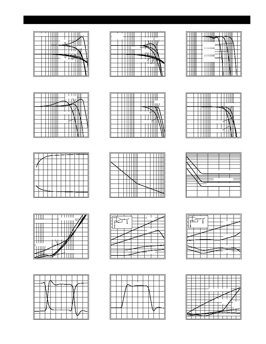
CLC417 Typical Performance Characteristics
(V
cc
= ±5V, A
v
= +2, R
L
= 100
; unless specified)
Frequency Response
Normalized Magnitude (1dB/div)
Frequency (MHz)
1
10
100
V
out
= 1V
pp
Phase (deg)
-90
-180
-450
-270
-360
0
A
v
= 1
A
v
= 1
A
v
= 2
A
v
= 2
A
v
= -1
A
v
= -1
Frequency Response vs. R
L
Magnitude (1dB/div)
Frequency (MHz)
1
10
100
Phase (deg)
-90
-180
-450
-270
-360
0
R
L
= 1k
R
L
= 1k
R
L
= 100
R
L
= 100
R
L
= 50
R
L
= 50
A
v
= +2
V
out
= 1V
pp
Frequency Response vs. C
L
Magnitude (1dB/div)
Frequency (MHz)
1
10
100
R
s
= 30.1
C
L
= 100pf
R
s
= 7.7
C
L
= 1000pf
R
s
= 80.6
C
L
= 10pf
Frequency Response vs. V
out
(A
v
= +1)
Magnitude (1dB/div)
Frequency (MHz)
1
10
100
V
o
= 0.2V
pp
V
o
= 4V
pp
V
o
= 2V
pp
Frequency Response vs. V
out
(A
v
= -1)
Magnitude (1dB/div)
Frequency (MHz)
1
10
100
V
o
= 0.2V
pp
V
o
= 4V
pp
V
o
= 2V
pp
Frequency Response vs. V
out
(A
v
= +2)
Magnitude (1dB/div)
Frequency (MHz)
1
10
100
V
o
= 0.2V
pp
V
o
= 4V
pp
V
o
= 2V
pp
Maximum Output Voltage vs. R
L
Maximum Output Voltage (V)
Load (
)
0
100
200
300
400
-4
-2
0
2
4
500
600
Recommended R
s
vs. Capacitive Load
R
s
(
)
C
L
(pF)
0
20
40
60
80
100
10
100
1000
Equivalent Input Noise
Noise Voltage (nV/
Hz)
Frequency (Hz)
100
10
1
1k
100
10k
100k
1M
10M
Noise Current (pA/
Hz)
100
10
1
Inverting Current = 12pA/
Hz
Voltage = 5nV/
Hz
Non-Inverting Current = 3pA/
Hz
2nd & 3rd Harmonic Distoration
Distortion Level (dBc)
Frequency (MHz)
1
10
-70
-80
-90
-60
-50
-40
V
o
= 2V
pp
3rd, R
L
= 100
2nd, R
L
= 100
2nd, R
L
= 1k
3rd, R
L
= 1k
2nd Harmonic Distortion vs. P
out
Distortion (dBc)
Output Power (dBm)
-90
-85
-80
-75
-70
-65
-60
-55
-10
-5
0
5
10
1MHz
500kHz
5MHz
10MHz
50
348
348
50
P
o
3rd Harmonic Distortion vs. P
out
Distortion (dBc)
Output Power (dBm)
-100
-90
-80
-70
-60
-50
-40
-10
-5
0
5
10
1MHz
500kHz
5MHz
10MHz
50
348
348
50
P
o
Small Signal Pulse Response
Output Voltage (V)
Time (5ns/div)
-0.08
-0.06
-0.04
-0.02
0
0.02
0.04
0.06
0.08
A
v
= +1
A
v
= -1
Large Signal Pulse Response
Output Voltage (V)
Time (5ns/div)
-2
-1
0
1
2
A
v
= +2
Differential Gain & Phase
Gain (%)
Number of 150
Loads
0
1
2
4
Phase (deg)
0
0.01
0.05
0.02
0.01
0.03
0.15
0.04
0.20
0.05
0.25
0.06
0.30
0.07
0.35
0.08
0.40
Phase Negative Sync
Phase
Positive
Sync
Gain Positive Sync
Gain Negative
Sync
3

http://www.national.com
4
CLC417 Typical Performance Characteristics
(V
cc
= ±5V, A
v
= +2, R
L
= 100
; unless specified)
CLC417 OPERATION
Description
The CLC417 is a dual current feedback buffer with the
following features:
s
Gains of +1, -1, and 2 are achievable without
external resistors
s
Differential gain and phase errors of 0.01%
and 0.03∞ into a 150
load
s
Low, 3.9mA, supply current per amplifier
The convenient 8-pin package and internal resistors
make common applications, like that seen on the front
page, easily feasible in a limited amount of space. The
professional video quality differential gain and phase
errors and low power capabilities of the CLC417 make
this product a good choice for video applications.
If gains other than +1, -1, or +2V/V are required, then the
CLC416 can be used. The CLC416 is a dual current
feedback amplifier with near identical performance, and
allows for external feedback and gain resistors.
Closed Loop Gain Selection
Gains of +1, +2, and -1V/V can be achieved by both of
the CLC417's amplifiers. Implement the gain selection
by connecting the inverting (-IN) and non-inverting (+IN)
pins as described in the table below.
The gain accuracy of the CLC417 is excellent and
stable over temperature. The internal feedback and gain
setting resistors, R
f
and R
g
, are diffused silicon resistors.
R
f
and R
g
have a process variation of ±20% and a
temperature coefficient of ~ 2000ppm/∞C. Although the
absolute values of R
f
and R
g
change with processing and
temperature, their ratio (R
f
/R
g
) remains constant. If an
external resistor is used in series with R
g
, gain accuracy
over temperature will be impacted by temperature coeffi-
cient differences between internal and external resistors.
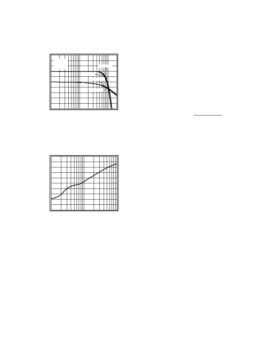
Non-Inverting Unity Gain Considerations
Gains of +1V/V are obtained by removing all resistive
and capacitive connections between the inverting
pins and ground on the CLC417 amplifiers. Too much
capacitive coupling between the inverting pin and ground
may cause stability problems. Minimize this capacitive
coupling by removing the ground plane near the
input and output pins. The response labeled
open in
Figure 1 is the result of the inverting pin left open and all
capacitive coupling removed. A flatter response can be
obtained by inserting a resistor between the
inverting and non-inverting pins as shown in Figure 2.
The two remaining plots in Figure 1 illustrate a 300
resistor and a short connected between pins 2 and 3 of
the CLC417.
Figure 1: Frequency Response vs.
Unity Gain Configuration
Figure 2: Optional Unity Gain Configuration
PSRR and CMRR
PSRR/CMRR (dB)
10k
100k
1M
Frequency (Hz)
10M
100M
60
50
40
30
20
10
PSRR
CMRR
Typical DC Errors vs. Temperature
Offset Voltage (mV)
Temperature (
∞
C)
6
5
4
1
-50
0
100
3
2
I
BN
Bias Current (
µ
A)
1
0
-1
-2
-3
50
I
BI
V
IO
Power Derating Curves
Power (W)
Ambient Temperature (
∞
C)
0.8
1.0
0.6
0
0
20
40
60
80
100
120 140
160 180
0.4
0.2
AJE
AJP
Magnitude (1dB/div)
Frequency (MHz)
1
100
Short
10
Open
R = 300
250
+
-
+
-
250
250
250
SMA
Input1
R
in
50
R
SMA
Output1
R
out
50
NOTE: The same technique can also
be applied to Channel B. Bypass
capacitors not shown.
Gain
Input Connections
A
v
+IN
-IN
-1V/V
ground
input signal
+1V/V
input signal
NC (open)
+2V/V
input signal
ground
5
http://www.national.com
Channel Matching
Channel matching and crosstalk efficiency are largely
dependent on board layout. The layout of National's dual
amplifier evaluation boards are optimized to produce
maximum channel matching and isolation. Typical
channel matching for the CLC417 is shown in Figure 3.
Figure 3: Channel Matching
The CLC417's channel-to-channel isolation is better than
70dB for input frequencies of 4MHz. Input referred
crosstalk vs. frequency is illustrated in Figure 4.
Figure 4: Input Referred Crosstalk vs. Frequency
Driving Cables and Capacitive Loads
When driving cables, double termination is used to
prevent reflections. For capacitive load applications, a
small series resistor at the output of the CLC417 will
improve stability. The
R
s
vs. Capacitive Load
plot, in the
Typical Performance section, gives the
recommended series resistance value for optimum
flatness at various capacitive loads.
Power Dissipation
The power dissipation of an amplifier can be described in
two conditions:
s
Quiescent Power Dissipation -
P
Q
(No Load Condition)
s
Total Power Dissipation -
P
T
(with Load Condition)
The following steps can be taken to determine the power
consumption for each CLC417 amplifier:
1. Determine the quiescent power
P
Q
= (V
CC
- V
EE
)
∑
I
CC
2. Determine the RMS power at the output stage
P
O
= (V
CC
- V
load
) (I
load
), where V
load
and I
load
are the RMS voltage and current across the
external load.
3. Determine the total RMS power
P
T
= P
Q
+ P
O
Add the total RMS powers for both channels to determine
the power dissipated by the dual.
The maximum power that the package can dissipate at a
given temperature is illustrated in the
Power Derating
curves in the
Typical Performance section. The power
derating curve for any package can be derived by utiliz-
ing the following equation:
where: T
amb
= Ambient temperature (∞C)
JA
= Thermal resistance, from junction to
ambient, for a given package (∞C/W)
Layout Considerations
A proper printed circuit layout is essential for achieving
high frequency performance. National provides
evaluation boards for the CLC417 (CLC730038 - DIP,
CLC730036 - SOIC) and suggests their use as a guide
for high frequency layout and as an aid for device testing
and characterization.
Supply bypassing is required for best performance. The
bypass capacitors provide a low impedance return
current path at the supply pins. They also provide high
frequency filtering on the power supply traces. Other
layout factors play a major role in high frequency
performance. The following are recommended as a basis
for high frequency layout:
1. Include 6.8
µ
F tantalum and 0.1
µ
F ceramic
capacitors on both supplies.
2. Place the 6.8
µ
F capacitors within 0.75 inches
of the power pins.
3. Place the 0.1
µ
F capacitors less than 0.1
inches from the power pins.
4. Remove the ground plane near the input
and output pins to reduce parasitic
capacitance.
5. Minimize all trace lengths to reduce series
inductances.
Additional information is included in the evaluation board
literature.
Special Evaluation Board Considerations
To optimize off-isolation of the CLC417, cut the R
f
trace
on both the 730038 and 730036 evaluation boards. This
cut minimizes capacitive feedthrough between the input
and output. Figure 5 indicates the alterations
recommended to improve off-isolation.
Magnitude (0.5dB/div)
Frequency (MHz)
1
10
100
A
v
= +2
R
L
= 100
V
o
= 2V
pp
Phase (deg)
-450
-360
-270
-180
-90
0
Channel A
Channel A
Channel B
Channel B
Crosstalk (dB)
Frequency (MHz)
-120
-100
-80
-60
-40
-20
1
100
10
P
(175
Tamb)
JA
=
∞ -