Features
s
130MHz bandwidth (A
v
= +2)
s
96mA output current
s
1.5mA supply current
s
-85/-75dBc HD2/HD3
s
15ns settling to 0.2%
s
-74dBc input-referred crosstalk (5MHz)
s
Single version available (CLC408)
Applications
s
ADSL/HDSL driver
s
Coaxial cable driver
s
UTP differential line driver
s
Transformer/coil driver
s
High capacitive-load driver
s
Video line driver
s
Portable/battery-powered line driver
s
Differential A/D driver
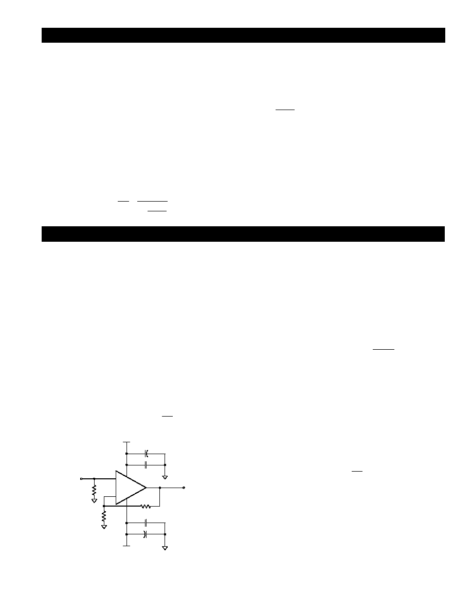
418 Pinout
V
o1
V
inv1
V
non-inv1
V
EE
V
o2
V
inv2
V
non-inv2
V
CC
+
-
1/2
CLC418
418 Typ App Diag
R
g2
+
V
o
-
-
+
R
t2
R
f2
R
f1
R
g1
1/2
CLC418
V
in
R
t1
R
m/2
R
m/2
R
L
Z
o
UTP
I
o
R
eq
I:n
V
d/2
-V
d/2
Typical Application Diagram
Differential Line Driver
with Load Impedance Conversion
Pinout
DIP & SOIC
General Description
The Comlinear CLC418 dual high-speed current-feedback
operational amplifier is designed to drive low-impedance and
high capacitance loads while maintaining high signal fidelity.
Operating on �5V power supplies, each of the CLC418's
amplifiers produces a continuous 96mA output current. Into a
back-terminated 50
load, the devices produce -85/-64dBc
second/third harmonic distortion (A
v
= +2, V
o
= 2V
pp
, f = 1MHz).
The CLC418's current-feedback architecture maintains consistent
performance over a wide range of gain and signal levels. DC gain
and bandwidth can be set independently. With proper resistor
selection, either maximally flat gain response or linear phase
response can be selected.
Requiring a mere 15mW quiescent power per amplifier, the
CLC418 offers superior performance-vs-power with a 130MHz
small-signal bandwidth, 350V/ms slew rate and quick 4.6ns
rise/fall times (2Vstep). The combination of low quiescent power,
high output current drive and high performance make the
CLC418 a great choice for many battery-powered personal
communication/computing systems.
Combining the CLC418's two amplifiers (shown below) results in
a powerful differential line driver for driving video signals over
unshielded twisted-pair (UTP). The CLC418 can also be used for
driving differential-input step-up transformers for applications
such as Asynchronous Digital Subscriber Lines (ADSL) or High-
Bit-Rate Digital Subscriber Lines (HDSL).
The CLC418's amplifiers make excellent low-power high-
resolution A-to-D converter drivers with their very fast 15ns set-
tling time (to 0.2%) and ultra-low -85/-75dBc harmonic distortion
(A
v
= +2, V
o
= 2V
pp
, f = 1MHz, R
L
= 1k
).
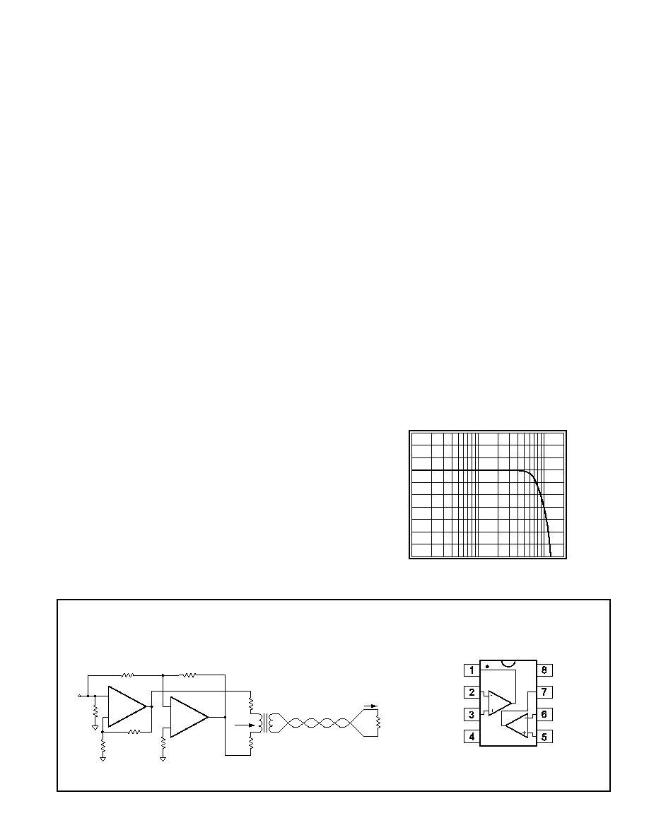
Non-Inverting Frequency Response
(A
v
= +2V/V, R
L
= 100
)
Normalized Magnitude (1dB/div)
Frequency (Hz)
418 Freq. Resp. Plot
10M
1M
100M
Comlinear CLC418
Dual High-Speed, Low-Power Line Driver
N
August 1996
Comlinear CLC418
Dual High-Speed, Low-Power Line Driver
� 1996 National Semiconductor Corporation
http://www.national.com
Printed in the U.S.A.

http://www.national.com
2
PARAMETERS
CONDITIONS
TYP
MIN/MAX RATINGS
UNITS
NOTES
Ambient Temperature
CLC418AJ
+25�C
+25�C
0 to 70�C
-40 to 85�C
FREQUENCY DOMAIN RESPONSE
-3dB bandwidth
V
o
< 1.0V
pp
130
80
80
75
MHz
B
V
o
< 4.0V
pp
45
33
29
28
MHz
-0.1dB bandwidth
V
o
< 1.0V
pp
30
25
20
20
MHz
gain flatness
V
o
< 1.0V
pp
peaking
DC to 200MHz
0
0.5
0.9
1.0
dB
B
rolloff
<30MHz
0.2
0.45
0.6
0.6
dB
B
linear phase deviation
<30MHz
0.2
0.4
0.5
0.5
deg
differential gain
NTSC, R
L
=150
0.1
�
�
�
%
differential phase
NTSC, R
L
=150
0.4
�
�
�
deg
TIME DOMAIN RESPONSE
rise and fall time
2V step
4.6
7.0
7.5
8.0
ns
settling time to 0.2%
2V step
15
30
38
40
ns
overshoot
2V step
5
12
12
12
%
slew rate
A
V
= +2
2V step
350
260
225
215
V/
�
s
DISTORTION AND NOISE RESPONSE
2
nd
harmonic distortion
2V
pp
, 1MHz
-85
�
�
�
dBc
2V
pp
, 1MHz; R
L
= 1k
-85
�
�
�
dBc
2V
pp
, 5MHz
-65
-60
-58
-58
dBc
B
3
rd
harmonic distortion
2V
pp
, 1MHz
-64
�
�
�
dBc
2V
pp
, 1MHz; R
L
= 1k
-75
�
�
�
dBc
2V
pp
, 5MHz
-50
-45
-44
-44
dBc
B
crosstalk (input-referred)
2V
pp
, 5MHz
-74
-68
-68
-68
dBc
equivalent input noise
voltage (e
ni
)
>1MHz
5
6.3
6.6
6.7
nV/
Hz
non-inverting current (i
bn
)
>1MHz
1.4
1.8
1.9
2.3
pA/
Hz
inverting current (i
bi
)
>1MHz
13
16
17
18
pA/
Hz
STATIC DC PERFORMANCE
input offset voltage
2
8
11
11
mV
A
average drift
25
�
35
40
�
V/�C
input bias current (non-inverting)
2
8
11
15
�
A
A
average drift
60
�
80
110
nA/�C
input bias current (inverting)
2
10
18
20
�
A
A
average drift
20
�
90
110
nA/�C
power supply rejection ratio
DC
55
50
48
48
dB
B
common-mode rejection ratio
DC
52
48
46
46
dB
supply current
R
L
=
, 2 channels
3.0
3.4
3.6
3.6
mA
A
MISCELLANEOUS PERFORMANCE
input resistance (non-inverting)
5
3
2.5
1
M
input capacitance (non-inverting)
1
2
2
2
pF
common mode input range
�2.7
�2.3
�2.2
�2.0
V
output voltage range
R
L
= 100
�3.3
�2.9
�2.8
�2.6
V
output voltage range
R
L
=
�4.0
�3.8
�3.7
�3.5
V
output current
96
96
96
60
mA
C
output resistance, closed loop
DC
0.03
0.15
0.2
0.3
CLC418 Electrical Characteristics
(A
V
= +2, R
f
= 1k
, V
cc
= + 5V, R
L
= 100
,
T = 25�C
;
unless specified)
Absolute Maximum Ratings
supply voltage
�7V
output current (see note C)
96mA
common-mode input voltage
�V
CC
maximum junction temperature
+175�C
storage temperature range
-65�C to +150�C
lead temperature (soldering 10 sec)
+300�C
ESD rating (human body model)
4000V
Notes
A) J-level: spec is 100% tested at +25�C, sample tested at +85�C.
L-level: spec is 100% wafer probed at +25�C.
B) J-level: spec is sample tested at +25�C.
C) The output current sourced or sunk by the CLC418 can
exceed the maximum safe output current limit.
2
Min/max ratings are based on product characterization and simulation. Individual parameters are tested as noted. Outgoing quality levels are
determined from tested parameters.

3
http://www.national.com
Typical Performance Characteristics
(A
v
= +2, R
f
= 1k
, R
L
= 100
, V
CC
= + 5V, T = 25�C
;
CLC418AJ; unless specified)
Non-Inverting Frequency Response
Normalized Magnitude (1dB/div)
Frequency (Hz)
408 Plot1
10M
Phase (deg)
-90
-180
-450
-270
-360
1M
100M
A
v
+1
A
v
+2
R
f
=953
A
v
+2
A
v
+5
R
f
=402
A
v
+5
A
v
+10
R
f
=200
A
v
+10
A
v
+1
R
f
=3k
0
V
o
= 1V
pp
Gain
Phase
Inverting Frequency Response
Normalized Magnitude (1dB/div)
Frequency (Hz)
408 Plot2
10M
Phase (deg)
0
-270
-360
-450
-90
-180
1M
100M
A
v
-1
A
v
-2
R
f
=681
A
v
-2
A
v
-5
R
f
=301
A
v
-5
A
v
-10
R
f
=200
A
v
-10
A
v
-1
R
f
=806
Gain
Phase
V
o
= 1V
pp
Frequency Response vs. R
L
Normalized Magnitude (1dB/div)
Frequency (Hz)
408 Plot3
10M
Phase (deg)
-90
-180
-450
-270
-360
1M
100M
R
L
=1k
R
f
=1.21k
R
L
=25
R
L
=100
R
L
=100
R
f
=1k
R
L
=1k
R
L
=25
R
f
=0.95k
0
Gain
Phase
V
o
= 1V
pp
Frequency Response vs. V
out
Normalized Magnitude (1dB/div)
Frequency (Hz)
408 Plot4
10M
1M
100M
0.10V
pp
2.0V
pp
4.0V
pp
1.0V
pp
Frequency Response vs. Capacitive Load
Magnitude (1dB/div)
Frequency (Hz)
408 Plot5
10M
1M
100M
C
L
=100pF
R
s
=24.9
C
L
=10pF
R
s
=100
C
L
= 1000pF
R
s
=5.7
C
L
1k
R
s
+
-
1k
1k
C
L
=0pF
R
s
=0
V
o
= 1V
pp
Small Signal Channel Matching
Normalized Magnitude (1dB/div)
Frequency (Hz)
418 Plot6
1M
10M
100M
V
o
= 1V
pp
Phase (deg)
-180
-225
-135
-90
-45
0
Channel A
Channel B
Channel A
Channel B
PSRR and CMRR
PSRR/CMRR (dB)
Frequency (Hz)
408 Plot7
60
50
20
10
0
1k
10k
100k
40
30
CMRR
1M
10M
100M
PSRR
Open Loop Transimpedance Gain, Z(s)
Magnitude (
)
Frequency (Hz)
418 Plot8
1M
100k
100
1k
10k
100M
10k
1k
Gain
Phase (deg)
180
140
20
100
60
Phase
100k
1M
10M
100
-
+
CLC418
V
o
I
i
Equivalent Input Noise
Noise Voltage (nV/
Hz)
Frequency (Hz)
408 Plot9
100
1
1k
10k
100M
10
i
bi
Noise Current (pA/
Hz)
100
10
1
100k
1M
10M
e
ni
i
bn
Input-Referred Crosstalk
Crosstalk (dB)
Frequency (Hz)
418 Plot10
-40
-60
-50
-90
1M
10M
100M
-70
-80
V
o
= 1V
pp
2nd & 3rd Harmonic Distortion
Distortion (dBc)
Frequency (Hz)
408 Plot10
-50
-40
-30
-20
-60
-90
1M
10M
-70
-80
2nd
R
L
= 1k
3rd
R
L
= 100
3rd
R
L
= 1k
2nd
R
L
= 100
V
o
= 2V
pp
2nd Harmonic Distortion, R
L
= 25
Distortion (dBc)
Output Amplitude (V
pp
)
408 Plot11
-55
-50
-45
-60
-75
0
1
5
-65
-70
1MHz
2
3
4
2MHz
5MHz
10MHz
3rd Harmonic Distortion, R
L
= 25
Distortion (dBc)
Output Amplitude (V
pp
)
408 Plot12
-40
-30
-20
-50
-80
0
1
5
-60
-70
1MHz
2
3
4
2MHz
5MHz
10MHz
2nd Harmonic Distortion, R
L
= 100
Distortion (dBc)
Output Amplitude (V
pp
)
408 Plot13
-90
-85
-80
-75
-70
-65
-60
-55
-50
0
1
5
1MHz
2
3
4
2MHz
5MHz
10MHz
3rd Harmonic Distortion, R
L
= 100
Distortion (dBc)
Output Amplitude (V
pp
)
408 Plot14
-80
-70
-60
-50
-40
-30
0
1
5
1MHz
2
3
4
2MHz
5MHz
10MHz

http://www.national.com
4
Typical Performance Characteristics
(A
v
= +2, R
f
= 1k
, R
L
= 100
, V
CC
= + 5V, T = 25�C
;
CLC418AJ; unless specified)
3rd Harmonic Distortion, R
L
= 1k
Distortion (dBc)
Output Amplitude (V
pp
)
408 Plot16
-95
-90
-85
-80
-75
-70
-65
-60
-55
0
1
5
1MHz
2
3
4
2MHz
5MHz
10MHz
2nd Harmonic Distortion, R
L
= 1k
Distortion (dBc)
Output Amplitude (V
pp
)
408 Plot15
-95
-90
-85
-80
-75
-70
-65
-60
0
1
5
1MHz
2
3
4
2MHz
5MHz
10MHz
Closed Loop Output Resistance
Output Resistance (
)
Frequency (Hz)
408 Plot17
100
0.1
10M
100M
10
1
Gain Flatness & Linear Phase Deviation
Magnitude (0.1dB/div)
Frequency (Hz)
408 Plot18
1M
10M
Gain
Phase Deviation (0.1
�
/div)
Phase
Small Signal Pulse Response
Output Voltage
Time (10ns/div)
408 Plot20
0.20
0.10
-0.20
0
-0.10
A
v
+2
A
v
-2
Large Signal Pulse Response
Output Voltage
Time (10ns/div)
408 Plot21
4.0
2.0
-4.0
0
-2.0
A
v
+2
A
v
-2
Pulse Crosstalk
Active Channel Output (1V/div)
Time (10ns/div)
418 Plot22
Active Output Channel
Other Channel Output (20mV/div)
Short Term Settling Time
V
o
(% Output Step)
Time (s)
408 Plot22
0.2
0.1
-0.2
0
20n
100n
0
-0.1
V
out
= 2V
step
40n
60n
80n
Long Term Settling Time
V
o
(% Output Step)
Time (s)
408 Plot23
0.4
-0.4
1
�
1m
1
0
10
�
100
�
10m
100m
-0.2
0.2
Settling Time vs. Capacitive Load
Settling Time (ns)
CL (F)
408 Plot24
70
60
30
20
10
100p
20p
1000p
50
40
Rs (
)
60
50
20
10
0
40
30
R
s
0.05%
0.1%
I
BI
, I
BN
, V
OS
vs. Temperature
Offset Voltage V
OS
(mV)
Temperature (
�
C)
408 Plot25
7.0
6.0
1.0
-50
0
100
5.0
4.0
3.0
2.0
V
OS
I
BI
, I
BN
(
�
A)
3.5
3.0
1.5
1.0
0.5
2.5
2.0
50
I
BI
I
BN
5
http://www.national.com
CLC418 OPERATION
The CLC418 has a current-feedback (CFB) architecture
built in an advanced complementary bipolar process.
The key features of current-feedback are:
s
AC bandwidth is independent of voltage gain
s
Inherently unity-gain stability
s
Frequency response may be adjusted with
feedback resistor (R
f
in Figures 1-3)
s
High slew rate
s
Low variation in performance for a wide range
of gains, signal levels and loads
s
Fast settling
Current-feedback operation can be explained with a
simple model. The voltage gain for the circuits in Figures 1
and 2 is approximately:
where:
s
A
v
is the DC voltage gain
s
R
f
is the feedback resistor
s
Z(j
) is the CLC418's open-loop
transimpedance gain
s
is the loop gain
The denominator of the equation above is approximately
1 at low frequencies. Near the -3dB corner
frequency, the interaction between R
f
and Z(j
)
dominates the circuit performance. Increasing R
f
does
the following:
s
Decreases loop gain
s
Decreases bandwidth
s
Reduces gain peaking
s
Lowers pulse response overshoot
s
Affects frequency response phase linearity
CLC418 DESIGN INFORMATION
Standard op amp circuits work with CFB op amps. There
are 3 unique design considerations for CFB:
s
The feedback resistor (R
f
in Figures 1-3) sets
AC performance
s
R
f
cannot be replaced with a short or a capacitor
s
The output offset voltage is not reduced by
balancing input resistances
The following sub-sections cover:
s
Design parameters, formulas and techniques
s
Interfaces
s
Application circuits
s
Layout techniques
s
SPICE model information
DC Gain (non-inverting)
The non-inverting DC voltage gain for the configuration
shown in Figure 1 is:
Figure 1: Non-Inverting Gain
The normalized gain plots in the
Typical Performance
Characteristics section show different feedback
resistors (R
f
) for different gains. These values of R
f
are
recommended for obtaining the highest bandwidth with
minimal peaking. The resistor R
t
provides DC bias for
the non-inverting input.
For A
v
< 6, use linear interpolation on the nearest A
v
values to calculate the recommended value of R
f
. For A
v
6, the minimum recommended R
f
is 200
.
Select R
g
to set the DC gain:
DC gain accuracy is usually limited by the tolerance of R
f
and R
g
.
DC Gain (unity gain buffer)
The recommended R
f
for unity gain buffers is 3k
. R
g
is
left open. Parasitic capacitance at the inverting node
may require a slight increase of R
f
to maintain a flat
frequency response.
DC Gain (inverting)
The inverting DC voltage gain for the configuration
shown in Figure 2 is:
The normalized gain plots in the
Typical Performance
Characteristics
section show different feedback
resistors (R
f
) for different gains. These values of R
f
are
recommended for obtaining the highest bandwidth with
minimal peaking. The resistor R
t
provides DC bias for
the non-inverting input.
For |A
v
| < 6, use linear interpolation on the nearest A
v
values to calculate the recommended value of R
f
. For
|A
v
|
6, the minimum recommended R
f
is 200
.
+
-
1/2
CLC418
418 Fig1
R
f
0.1
�
F
6.8
�
F
V
o
V
in
V
CC
0.1
�
F
6.8
�
F
V
EE
3(5)
2(6)
4
8
1(7)
+
+
R
g
R
t
V
V
A
1
R
Z j
o
in
v
f
=
+
( )
Z j
R
f
( )
A
1
R
R
v
f
g
= +
R
R
A
1
g
f
v
=
-
A
R
R
v
f
g
= -