 | –≠–ª–µ–∫—Ç—Ä–æ–Ω–Ω—ã–π –∫–æ–º–ø–æ–Ω–µ–Ω—Ç: CLC420 | –°–∫–∞—á–∞—Ç—å:  PDF PDF  ZIP ZIP |
CLC420
High-Speed, Voltage Feedback Op Amp
General Description
The CLC420 is an operational amplifier designed for applica-
tions requiring matched inputs, integration or transimped-
ance amplification. Utilizing voltage feedback architecture,
the CLC420 offers a 300MHz bandwidth, a 1100V/µs slew
rate and a 4mA supply current (power consumption of
40mW,
±
5V supplies).
Applications such as differential amplifiers will benefit from
70dB common mode rejection ratio and an input offset cur-
rent of 0.2µA. With its unity-gain stability, 2pA/
current
noise and 3µA of input bias current, the CLC420 is designed
to meet the needs of filter applications and log amplifiers.
The low input offset current and current noise, combined
with a settling time of 18ns to 0.01% make the CLC420 ideal
for D/A converters, pin diode receivers and photo multipliers
amplifiers. All applications will find 70dB power supply rejec-
tion ratio attractive.
Features
n
300MHz small signal bandwidth
n
1100V/µs slew rate
n
Unity-gain stability
n
Low distortion, -60dBc at 20MHz
n
0.01% settling in 18ns
n
0.2µA input offset current
n
2pA
current noise
Applications
n
Active filters/integrators
n
Differential amplifiers
n
Pin diode receivers
n
Log amplifiers
n
D/A converters
n
Photo multiplier amplifiers
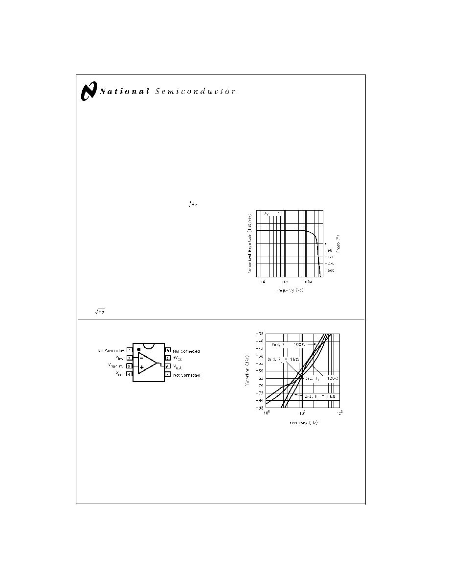
Connection Diagram
Non-Inverting Frequency Response
DS012752-19
DS012752-18
Pinout
DIP & SOIC
DS012752-20
2nd and 3rd Harmonic Distortion
September 1999
CLC420
High-Speed,
V
oltage
Feedback
Op
Amp
© 1999 National Semiconductor Corporation
DS012752
www.national.com
Ordering Information
Package
Temperature Range
Industrial
Packaging
Marking
NSC
Drawing
8-pin plastic DIP
-40∞C to +85∞C
CLC420AJP
N08E
8-pin plastic SOIC
-40∞C to +85∞C
CLC420AJE
CLC420AJE-TR13
M08A
CLC420
www.national.com
2
Absolute Maximum Ratings
(Note 1)
If Military/Aerospace specified devices are required,
please contact the National Semiconductor Sales Office/
Distributors for availability and specifications.
Supply Voltage (V
CC
)
±
7V
I
OUT
(is short circuit protected to ground,
but maximum reliability will be
maintained if I
OUT
does not exceed
70mA, except A8D, B8D which should
not exceed 35mA over the military
temperature range)..
Common Mode Input Voltage
±
V
CC
Differential Input Voltage
10V
Junction Temperature
+150∞C
Operating Temperature Range
AJ:
-40∞C to +85∞C
Storage Temperature Range
-65∞C to +150∞C
Lead Solder Duration (+300∞C)
10 sec
Electrical Characteristics
A
V
=+1, V
CC
=
±
5V, R
L
=100
, R
f
= 0
; unless specified
Symbol
Parameter
Conditions
Typ
Max/Min (Note 2)
Units
Ambient Temperature
CLC420AJ
+25∞C
-40∞C
+25∞C
+85∞
Frequency Domain Response
SSBW
-3dB bandwidth
V
OUT
<
0..4V
PP
300
>
200
>
200
>
130
MHz
LSBW
V
OUT
<
5V
PP
40
>
20
>
25
>
20
MHz
SSBWI
A
v
=-1, R
f
=500
V
OUT
<
0.4V
PP
100
>
65
>
65
>
45
MHz
LSBWI
A
v
=-1, R
f
=500
V
OUT
<
5V
PP
60
>
30
>
35
>
30
MHz
gain flatness
V
OUT
<
0.4V
PP
GFPL
peaking
0.1MHz to
100MHz
0
<
1
<
0.6
<
0.6
dB
GFPH
peaking
>
100MHz
0
<
5
<
3
<
3
dB
GFR
rolloff
0.1MHz to
100MHz
0.2
<
1
<
1
<
2
dB
GFRI
rolloff, A
v
=-1, R
f
=500
0.1MHz to
30MHz
0.2
<
1.4
<
1.4
<
1.6
dB
LPD
linear phase deviation
0.1MHz to
100MHz
0.9
<
1.8
<
1.8
<
2.5
∞
Time Domain Response
TRS
rise and fall time
0.4V step
1.2
<
2
<
2
<
3
ns
TRL
5V step
1.4
<
25
<
20
<
20
ns
TRSI
rise and fall time,A
v
=-1,
R
f
=500
0.4V step
3.5
<
5.5
<
5.5
<
7.8
ns
TRLI
5V step
6
<
10
<
9.5
<
10
ns
TSS
settling time to
±
0.1%
2V step
12
<
18
<
18
<
18
ns
TSP
±
0.01%
2V step
18
<
25
<
25
<
25
ns
OS
overshoot
0.4V step
8
<
35
<
25
<
25
%
SR
slew rate, A
v
=+2
5V step
1100
>
600
>
750
>
600
V/µs
SRI
slew rate, A
v
=-1, R
f
=500
5V step
750
>
430
>
500
>
430
V/µs
Distortion And Noise Response
HD2
2nd harmonic distortion
2V
PP
, 20MHz
-50
<
-40
<
-40
<
-40
dBc
HD3
3rd harmonic distortion
2V
PP
, 20MHz
-53
<
-45
<
-45
<
-40
dBc
HD2
2nd harmonic distortion
A
v
=-1 2V
PP
,
20MHz, R
f
=500
-51
<
-40
<
-40
<
-40
dBc
HD3
3rd harmonic distortion
A
v
=-1,
R
f
=500
2V
PP
,
20MHz, R
f
=500
-51
<
-40
<
-40
<
-35
dBc
input referred noise
VN
voltage
1MHz to
200MHz
4.2
<
5.3
<
5.3
<
6
nV/
CLC420
www.national.com
3
Electrical Characteristics
(Continued)
A
V
=+1, V
CC
=
±
5V, R
L
=100
, R
f
= 0
; unless specified
Symbol
Parameter
Conditions
Typ
Max/Min (Note 2)
Units
Distortion And Noise Response
ICN
current
1MHz to
200MHz
2
<
2.9
<
2.6
<
2.3
pA/
Static DC Performance
VIO
input offset voltage (Note 3)
1
<
3.2
<
2
<
3.5
mV
DVIO
average temperature coefficient
8
<
15
-
<
15
µV/∞C
IB
input bias current (Note 3)
3
<
20
<
10
<
10
µA
DIB
average temperature coefficient
45
<
120
-
<
60
A/∞C
IIO
input offset current (Note 3)
0.2
<
2.6
<
1
<
2
µA
DIIO
average temperature coefficient
2
<
20
-
<
10
nA/∞C
AOL
open loop gain (Note 3)
65
>
52
>
56
>
56
µA
PSRR
power supply rejection ratio
70
>
55
>
60
>
60
dB
CMRR
common mode rejection ratio
80
>
60
>
65
>
65
dB
ICC
supply current (Note 3)
no
load,quiescent
4
<
5
<
5
<
5
mA
Miscellaneous Performance
RIND
differential mode input
resistance
2
>
0.5
>
1
>
1
M
CIND
capacitance
1
<
2
<
2
<
2
pF
RINC
common mode input
resistance
1
>
0.25
>
0.5
>
0.5
M
CINC
capacitance
1
<
2
<
2
<
2
pF
RO
output impedence
at DC
0.02
<
0.3
<
0.2
<
0.2
VO
output voltage range
no load
±
3.6
±
2.8
±
3
±
3
V
VOL
output voltage range
RL=100
±
2.9
±
2.5
±
2.5
±
2.5
V
CMIR
common mode input range
for rated
performance
±
3.2
±
2.5
±
2.8
±
2.8
V
IO
output current
±
60
±
30
±
50
±
50
mA
Package Thermal Resistance
junction
to
case
CLC420AJP
65∞
-
-
-
-
C/W
junction
to
ambient
CLC420AJP
120∞
-
-
-
-
C/W
junction
to
case
CLC420AJE
60∞
-
-
-
-
C/W
junction
to
ambient
CLC420AJE
140∞
-
-
-
-
C/W
Note 1: "Absolute Maximum Ratings" are those values beyond which the safety of the device cannot be guaranteed. They are not meant to imply that the devices
should be operated at these limits. The table of "Electrical Characteristics" specifies conditions of device operation.
Note 2: Max/min ratings are based on product characterization and simulation. Individual parameters are tested as noted. Outgoing quality levels are determined
from tested parameters.
Note 3: AJ-level: spec. is 100% tested at +25∞C.
CLC420
www.national.com
4

Typical Performance Characteristics
Non-Inverting Frequency Response
DS012752-1
Inverting Frequency Response
DS012752-2
Frequency Response for Various
R
L
S
DS012752-3
Open Loop Gain and Phase
DS012752-4
Bandwidth vs. Gain,
Transimpedance Configuration
DS012752-5
2nd and 3rd Harmonic Distortion
DS012752-6
2-Tone, 3rd Order Intermodulation
Intercept
DS012752-7
Equivalent Input Noise
DS012752-8
PSRR, CMRR, and Closed Loop R
O
DS012752-9
CLC420
www.national.com
5