 | –≠–ª–µ–∫—Ç—Ä–æ–Ω–Ω—ã–π –∫–æ–º–ø–æ–Ω–µ–Ω—Ç: CLC423 | –°–∫–∞—á–∞—Ç—å:  PDF PDF  ZIP ZIP |
Features
s
Single +5V supply
s
Input includes V
EE
s
94MHz unity-gain bandwidth
s
-74/-94dBc HD2/HD3
s
60mA output current
s
7.5ns rise/fall time (1V
pp
)
s
46ns settling time to 0.1%
Applications
s
Video ADC driver
s
Desktop multimedia
s
Single supply cable driver
s
Instrumentation
s
Video cards
s
Wireless IF amplifiers
s
Telecommunications
General Description
The Comlinear CLC423 is a wideband voltage-feedback
operational amplifier that is uniquely designed to provide high
performance from a single power supply. The CLC423 provides
near rail-to-rail operation and the common-mode input range
includes the negative rail. The CLC423 offers plenty of head-
room for single-supply applications as evidenced by its 4.3V
pp
output voltage from a single 5V supply.
Fabricated with a high-speed complementary bipolar process, the
CLC423 delivers a wide 94MHz unity-gain bandwidth, 7.5ns
rise/fall time and 150V/
µ
s slew rate. For single supply applications
such as video distribution or desktop multimedia, the CLC423
offers low 0.35%, 0.55∞ differential gain and phase errors.
The CLC423 provides high signal fidelity with -74/-94dBc 2nd/3rd
harmonics (1V
pp
, 1MHz, R
L
=150
). Combining this high fidelity
performance with CLC423's quick 46ns settling time to 0.1%
makes it an excellent choice for ADC buffering.
With its traditional voltage-feedback architecture and high-speed
performance, the CLC423 is the perfect choice for composite
signal conditioning circuit functions such as active filters,
integrators, differentiators, simple gain blocks and buffering.
V
in
50
250
+
-
250
0.1
µ
F
6.8
µ
F
150
NOTE: V
in
= 0.15V to 2.3V
CLC423
V
o
+5V
+
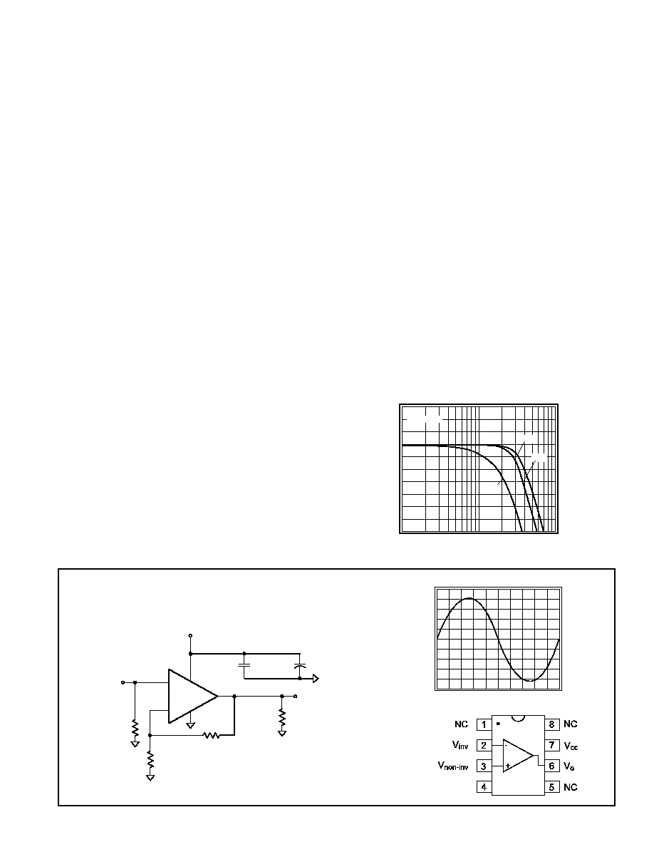
Typical Application
Single +5V Supply operation
Comlinear CLC423
94MHz, Single Supply Voltage Feedback Op Amp
Frequency Response vs. V
out
Magnitude (1dB/div)
Frequency (MHz)
1
10
100
1V
pp
2V
pp
4V
pp
A
v
= +2V/V
V
EE
Pinout
DIP & SOIC
Single Supply Response
Output Voltage (V)
Time (100ns/div)
V
EE
0
1
2
3
4
V
CC
5
August 1996
Comlinear CLC423
94MHz, Single Supply V
oltage Feedback Op
Amp
N
© 1996 National Semiconductor Corporation
http://www.national.com
Printed in the U.S.A.
http://www.national.com
2
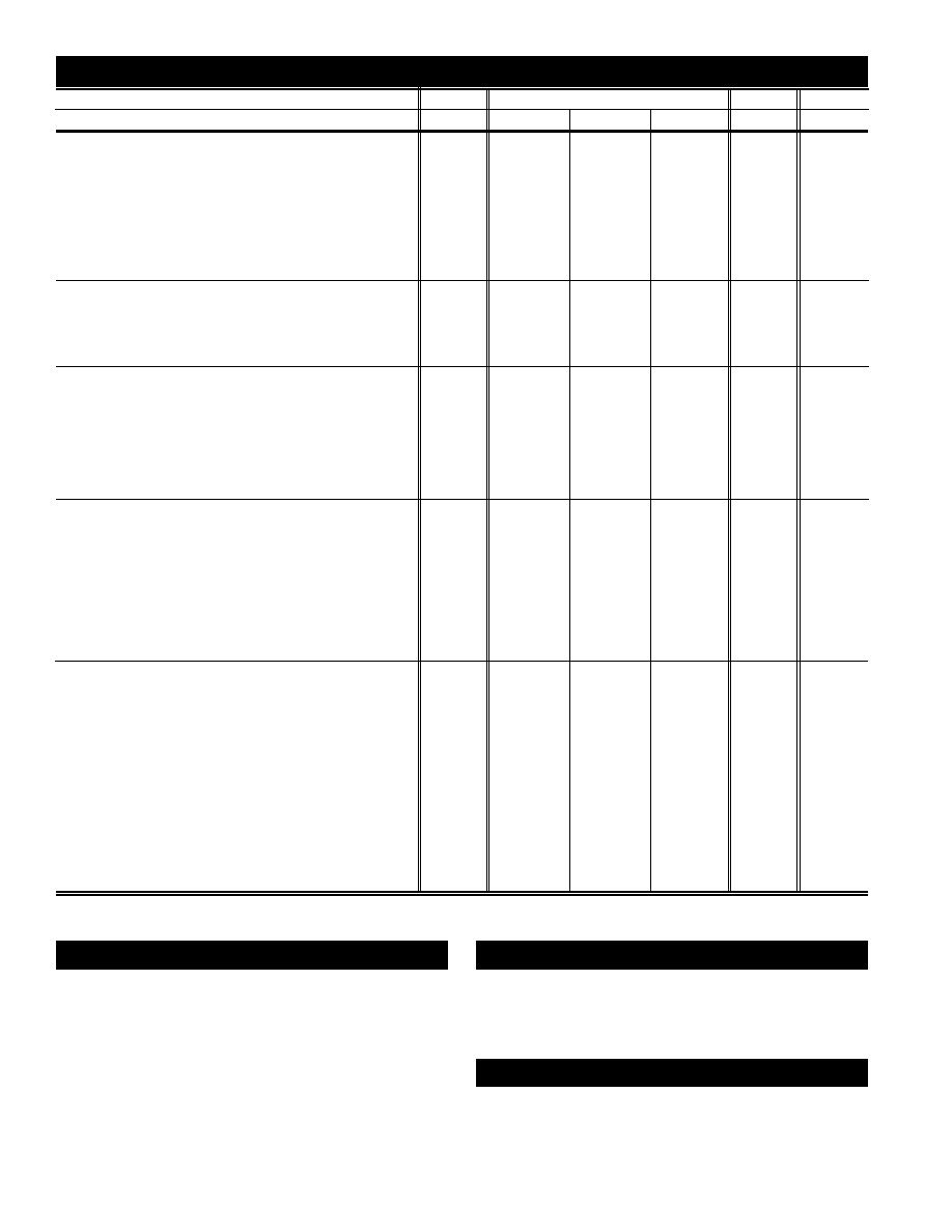
PARAMETERS
CONDITIONS
TYP
MIN/MAX RATINGS
UNITS
NOTES
CLC423AJ
25∞
25∞
0∞ to +70∞
-40∞ to +85∞
FREQUENCY DOMAIN RESPONSE
-3dB bandwidth
V
o
< 1.0V
pp
48
32
28
27
MHz
B
-3dB bandwidth
V
o
< 3.0V
pp
26
16
14
11
MHz
-3dB bandwidth A
V
= +1V/V
V
o
< 1.0V
pp
94
MHz
rolloff
<10MHz
0.1
0.5
0.7
0.8
dB
B
peaking
DC to 200MHz
0
0.5
0.7
0.8
dB
B
linear phase deviation
<15MHz
0.3
0.6
0.8
0.9
deg
differential gain
NTSC, R
L
=150
0.35
0.7
≠
≠
%
2
differential phase
NTSC, R
L
=150
0.55
2
≠
≠
deg
2
TIME DOMAIN RESPONSE
rise and fall time
1V step
7.5
13
14
16
ns
settling time to 0.1%
1V step
46
70
≠
≠
ns
overshoot
1V step
5
13
≠
≠
%
slew rate
A
V
= +2
2V step
150
90
83
65
V/
µ
s
DISTORTION AND NOISE RESPONSE
2
nd
harmonic distortion
1V
pp
, 1MHz
74
≠
≠
≠
-dBc
1V
pp
, 5MHz
62
55
52
52
-dBc
B
3
rd
harmonic distortion
1V
pp
, 1MHz
94
≠
≠
≠
-dBc
1V
pp
, 5MHz
75
65
63
62
-dBc
B
equivalent input noise
voltage
>1MHz
10
12.5
13.6
14
nV/
Hz
current
>1MHz
4
5
5.5
5.7
pA/
Hz
STATIC DC PERFORMANCE
input offset voltage
2
7
8
10
mV
A
average drift
4
≠
22
35
µ
V/∞C
input bias current
17
30
36
45
µ
A
A
average drift
80
≠
145
175
nA/∞C
input offset current
0.2
5
6
7.5
µ
A
average drift
10
≠
22
27
nA/∞C
power supply rejection ratio
DC
82
65
64
60
dB
B
common-mode rejection ratio
DC
82
55
53
50
dB
supply current
no load
7
8.5
8.5
8.5
mA
A
MISCELLANEOUS PERFORMANCE
input capacitance
1
2
2
2
pF
input resistance
700
500
450
360
k
output impedance
@DC
0.07
0.15
0.24
0.7
input voltage range, high
3.7
3.45
3.25
3.15
V
input voltage range, low
0
0
0
0
V
output voltage range, high
R
L
= 150
4.5
4.35
4.3
4.2
V
output voltage range, low
R
L
= 150
0.35
0.5
0.5
0.55
V
output voltage range, high
no load
4.8
4.6
4.55
4.45
V
output voltage range, low
no load
0.45
0.65
0.7
0.75
V
output current
source
60
50
40
34
mA
output current
sink
36
20
16
10
mA
supply voltage, maximum
7
7
7
V
1
supply voltage, minimum
4
4
4
V
1
Electrical Characteristics
(V
s
= +5V
1
, V
cm
= +2.5V, A
v
= +2, R
f
= 250
W,
R
L
= 150
W
to GND; unless specified)
Absolute Maximum Ratings
supply voltage (V
s
)
+7V
I
out
is short circuit protected to ground
common-mode input voltage
V
EE
to V
CC
maximum junction temperature
+175∞C
storage temperature range
-65∞C to +150∞C
lead temperature (soldering 10 sec)
+260∞C
differential input voltage
±2V
EDS tolerance (Note 3)
4000V
Notes
A) J-level: spec is 100% tested at 25∞C, sample tested at 85∞C.
B) J-level: spec is sample tested at 25∞C.
1) V
s
= V
CC
≠ V
EE
.
2) Tested with R
L
tied to +2.5V.
3) Human body model, 1.5k
in series with 100pF.
Reliability Information
transistor count
62
MTBF
823Mhr
Min/max ratings are based on product characterization and simulation. Individual parameters are tested as noted. Outgoing quality levels are
determined from tested parameters.

3
http://www.national.com
Typical Performance Characteristics
(V
s
= +5V
1
, V
cm
= +2.5V, A
v
= +2, R
f
= 250
W,
R
L
= 150
W
to GND; unless specified)
Non-Inverting Frequency Response
Magnitude (1dB/div)
Frequency (MHz)
1
10
100
A
v
= 1
R
f
= 0
Phase (deg)
-225
-180
-135
-90
-45
0
A
v
= 2
A
v
= 4
A
v
= 10
A
v
= 10
A
v
= 4
A
v
= 2
A
v
= 1
V
o
= 0.25V
pp
Inverting Frequency Response
Magnitude (1dB/div)
Frequency (MHz)
1
10
100
A
v
= -1
Phase (deg)
-45
0
45
90
135
180
A
v
= -2
A
v
= -5
A
v
= -10
A
v
= -10
A
v
= -5
A
v
= -2
A
v
= -1
V
o
= 0.25V
pp
Frequency Response vs. R
L
Magnitude (1dB/div)
Frequency (MHz)
0
10
100
R
L
= 1k
Phase (deg)
-225
-180
-135
-90
-45
0
45
90
135
180
225
R
L
= 150
R
L
= 75
R
L
= 75
R
L
= 150
R
L
= 1k
V
o
= 0.25V
pp
Frequency Response vs. V
out
Magnitude (1dB/div)
Frequency (MHz)
1
10
100
V
o
= 4V
pp
V
o
= 2V
pp
V
o
= 0.25V
pp
V
o
= 1V
pp
Frequency Response vs. C
L
Magnitude (1dB/div)
Frequency (MHz)
1
10
100
C
L
= 10pF
R
s
= 249
C
L
= 1000pF
R
s
= 22
C
L
= 100pF
R
s
= 54.9
1k
250
250
R
s
C
L
Open Loop Gain & Phase
Open Loop Gain (dB)
Frequency (MHz)
0.001
0.01
0.1
1
10
100
Phase (deg)
-120
Gain
-20
-100
0
-80
20
-60
40
-40
60
-20
80
0
100
Phase
Harmonic Distortion vs. Frequency
Distortion (dBc)
Frequency (MHz)
0.1
1
10
2nd
R
L
= 150
-100
-90
-80
-70
-60
-50
3rd
R
L
= 150
3rd
R
L
= 1k
2nd
R
L
= 1k
V
o
= 1V
pp
2nd Harmonic Distortion vs. V
out
Distortion (dBc)
Output Amplitude (V
pp
)
0
1
2
3
4
R
L
= 150
-80
-70
-60
-50
-40
-30
10MHz
5MHz
2MHz
1MHz
0.1MHz
-90
3rd Harmonic Distortion vs. V
out
Distortion (dBc)
Output Amplitude (V
pp
)
0
1
2
3
4
R
L
= 150
-80
-70
-60
-50
-40
-30
10MHz
5MHz
2MHz
1MHz
0.1MHz
-90
-100
Small Signal Pulse Response
Output Voltage (0.05V/div)
Time (20ns/div)
Large Signal Pulse Response
Output Voltage (0.5V/div)
Time (20ns/div)
Equivalent Input Noise
Voltage Noise (nV/Hz)
Frequency (MHz)
0.001
0.1
10
Current Noise (pA/Hz)
1
Voltage = 9.5nV/
Hz
1
10
10
100
100
1
0.01
Current = 3.2pA/
Hz
I
B
, V
IO
, vs. Temperature
V
IO
(mV)
Temperature (
∞
C)
-40
-20
0
20
40
60
I
B
(
µ
A)
-22
I
B
0.5
-20
0.7
-18
0.9
-16
1.1
-14
1.3
-12
1.5
-10
1.7
V
IO
80
Differential Gain and Phase (3.58MHz)
Gain (%)
Number of 150
Loads
1
2
3
4
Phase (deg)
0
0
0.5
0.5
1
1
1.5
1.5
2
2
2.5
2.5
Phase Neg Sync
Gain Neg Sync
R
L
tied to +2.5V
PSRR, CMRR & Linear R
out
vs. Frequency
PSRR, CMRR (dB)
Frequency (MHz)
0.001
0.01
0.1
1
Output Resistance (
)
0
0
5
20
10
40
15
60
20
80
25
100
10
PSRR
R
out
CMRR
http://www.national.com
4
CLC423 OPERATIONS
Description
The CLC423 is a voltage feedback amplifier designed for
single supply operation. The CLC423 is a single version
of the CLC427 with the following features:
s
Operates from a single +5V supply
s
Maintains near rail-to-rail performance
s
Includes the negative rail (0V) in the Common
Mode Input Range (CMIR)
s
Offers low -74/-94dBc 2nd and 3rd harmonic
distortion
s
Provides BW > 20MHz and 1MHz distortion
< -50dBc at V
o
= 4V
pp
Single Supply Operation (V
CC
= +5V, V
EE
= GND)
The CLC423 is designed to operate from 0 and 5V
supplies. The specifications given in the
Electrical
Characteristics table are measured with a common
mode voltage (V
cm
) of 2.5V. V
cm
is the voltage around
which the inputs are applied and the output voltages are
specified.
Operating from a single +5V supply, the CMIR of the
CLC423 is typically 0V to +3.7V. The typical output range
with R
L
= 150
is +0.35V to +4.5V.
For DC coupled single supply operation, it is recom-
mended that input signal levels remain above ground.
For input signals that drop below ground, AC coupling
and level shifting the signal are possible remedies.
For input signals that remain above ground, no
adjustments need to be made. The non-inverting and
inverting configurations for both input conditions are
illustrated in the following 2 sections.
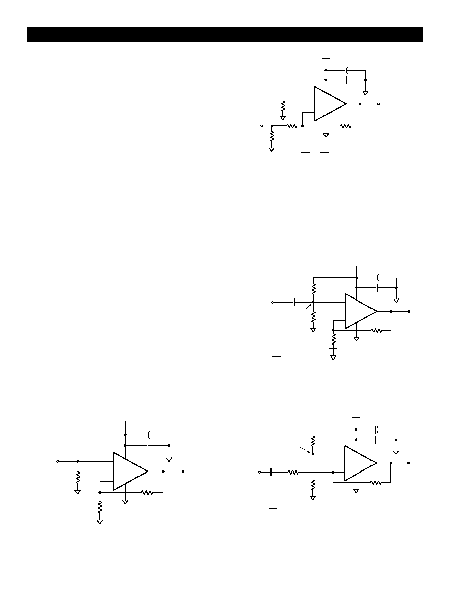
DC Coupled Single Supply Operation
Figures 1 and 2 show the recommended non-inverting
and inverting configurations for purely positive input
signals.
Figure 1: Non-inverting Configuration
Figure 2: Inverting Configuration
AC Coupled Single Supply Operation
Figures 3 and 4 show possible non-inverting and
inverting configurations for input signals that go below
ground. The input is AC coupled to prevent the need
for level shifting the input signal at the source. The
resistive voltage divider biases the non-inverting input to
V
CC
˜ 2 = 2.5V.
Figure 3: AC Coupled Non-inverting Configuration
Figure 4: AC Coupled Inverting Configuration
+
-
CLC423
R
f
0.1
µ
F
6.8
µ
F
V
o
V
in
+5V
R
g
R
t
3
2
4
7
6
V
V
1
R
R
o
in
f
g
= +
+
CLC423
3
2
7
6
+
-
R
f
0.1
µ
F
6.8
µ
F
V
o
V
in
+5V
R
b
4
R
g
R
t
V
V
R
R
o
in
f
g
= -
Select R to yield
desired R
R || R
t
in
t
g
=
+
3
2
7
6
CLC423
+
-
R
f
0.1
µ
F
6.8
µ
F
V
o
V
in
+5V
R
g
R
4
C
C
c
R
+
V
V
1
R
R
2.5
o
in
f
g
=
+
+
low frequency cutoff
1
2 R C
, where: R
R
2
in
c
in
=
=
2.5V
R
R
source
>>
R C
RC
g
c
>>
CLC423
3
2
7
6
+
-
R
f
0.1
µ
F
6.8
µ
F
V
o
V
in
+5V
R
4
C
c
R
+
V
V
R
R
2.5
o
in
f
g
=
-
+
low frequency cutoff
1
2 R C
g
c
=
2.5V
R
g
5
http://www.national.com
Load Termination
Since the CLC423 design has been optimized for Single
Supply Operation, it is more capable of sourcing rather
than sinking current. For optimum performance, the load
should be tied to V
EE
. When the load is tied to V
EE
, the
output always sources current.
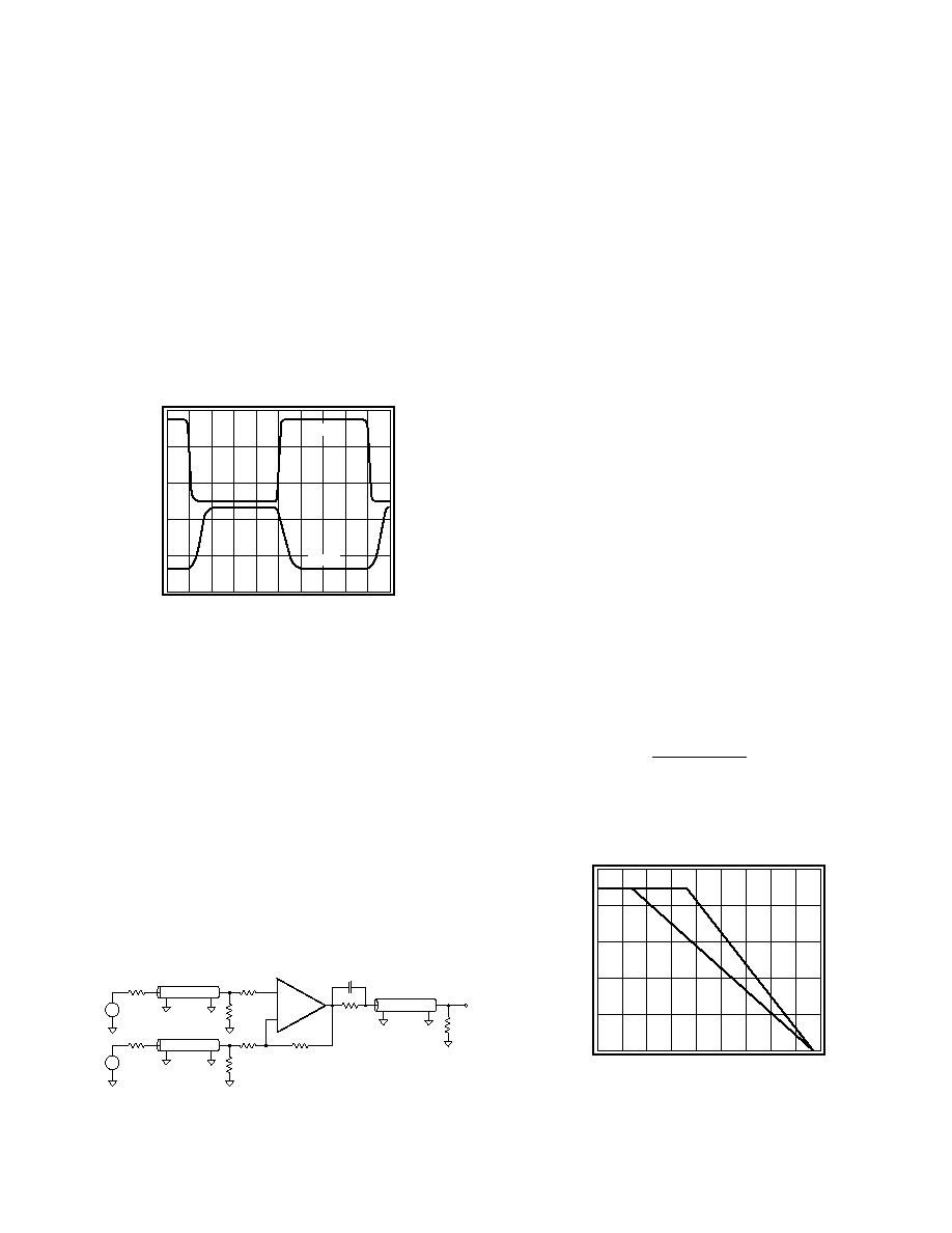
Output Overdrive Recovery
When the output range of an amplifier is exceeded, time
is required for the amplifier to recover from this over
driven condition. Figure 5 illustrates the overload
recovery of the CLC423 when the output is overdriven.
An input was applied in an attempt to drive the output to
twice the supply rails (2
∑
(V
CC
-V
EE
) = 10V), but the
output limits. An inverting gain topolgy was used, see
Figure 2. As indicated, the CLC423 recovers within
25ns on the rising edge and within 10ns on the falling
edge.
Figure 5: Overdrive Recovery
Driving Cables and Capacitive Loads
When driving cables, double termination is used to
prevent reflections. For capacitive load applications, a
small series resistor at the output of the CLC423
will improve stability and settling performance. The
Frequency Response vs. C
L
plot, in the typical
performance section, gives the recommended series
resistance value for optimum flatness at various
capacitive loads.
Transmission Line Matching
One method for matching the characteristic impedance
(Z
o
) of a transmission line or cable is to place the
appropriate resistor at the input or output of the amplifier.
Figure 6 shows typical inverting and non-inverting circuit
configurations for matching transmission lines.
Figure 6: Transmission Line Matching
Non-inverting gain applications:
s
Connect R
g
directly to ground.
s
Make R
1
, R
2
, R
6
, and R
7
equal to Z
o
.
s
Use R
3
to isolate the amplifier from reactive
loading caused by the transmission line, or
by parasitics.
Inverting gain applications:
s
Connect R
3
directly to ground.
s
Make the resistors R
4
, R
6
, and R
7
equal to Z
o
.
s
Make R
5
II R
g
= Z
o
.
The input and output matching resistors attenuate the
signal by a factor of 2, therefore additional gain is
needed. Use C
6
to match the output transmission line
over a greater frequency range. C
6
compensates for the
increase of the amplifier's output impedance with
frequency.
Power Dissipation
Follow these steps to determine the power consumption
of the CLC423:
1. Calculate the quiescent (no-load) power:
P
amp
= I
CC
(V
CC
- V
EE
)
2. Calculate the RMS power at the output stage:
P
o
= (V
CC
- V
load
) (I
load
), where V
load
and
I
load
are the RMS voltage and current across
the external load.
3. Calculate the total RMS power:
P
t
= P
amp
+ P
o
The maximum power that the DIP and SOIC packages
can dissipate at a given temperature is illustrated in
Figure 7. The power derating curve for any package can
be derived by utilizing the following equation:
where:
T
amb
= Ambient temperature (∞C)
ja = Thermal resistance, from junction to ambient, for a
given package (∞C/W)
Figure 7: Power Derating Curves
p
Input Voltage (4V/div)
Time (50ns/div)
Output Voltage (2V/div)
Input
Output
CLC423
+
-
Fi
R
3
Z
0
R
6
V
o
Z
0
R
1
R
2
+
-
R
g
Z
0
R
4
R
5
V
1
V
2
+
-
R
f
C
6
R
7
Power (W)
Ambient Temperature (
∞
C)
0
0.2
0.4
0.6
0.8
1.0
0
20
40
60
80
100 120 140 160 180
AJP
AJE
(175
T
amb
JA
∞ -
)