 | –≠–ª–µ–∫—Ç—Ä–æ–Ω–Ω—ã–π –∫–æ–º–ø–æ–Ω–µ–Ω—Ç: CLC425 | –°–∫–∞—á–∞—Ç—å:  PDF PDF  ZIP ZIP |
N
CLC425
Ultra Low Noise Wideband Op Amp
©
1999 National Semiconductor
Corporation
http://www.national.com
Printed in the U.S.A.
General Description
The CLC425 combines a wide bandwidth (1.9GHz GBW) with very
low input noise (1.05nV/
Hz, 1.6pA/
Hz) and low dc errors (100
µµ
µµ
µ
V
V
OS
, 2
µµ
µµ
µ
V/∞C drift) to provide a very precise, wide dynamic-range
op amp offering closed-loop gains of
10.
Singularly suited for very wideband high-gain operation, the CLC425
employs a traditional voltage-feedback topology providing all the
benefits of balanced inputs, such as low offsets and drifts, as well
as a 96dB open-loop gain, a 100dB CMRR and a 95dB PSRR.
The CLC425 also offers great flexibility with its externally adjustable
supply current, allowing designers to easily choose the optimum
set of power, bandwidth, noise and distortion performance.
Operating from ±5V power supplies, the CLC425 defaults to a
15mA quiescent current, or by adding one external resistor, the
supply current can be adjusted to less than 5mA.
The CLC425's combination of ultra-low noise, wide gain-band-
width, high slew rate and low dc errors will enable applications in
areas such as medical diagnostic ultrasound, magnetic tape & disk
storage, communications and opto-electronics to achieve maximum
high-frequency signal-to-noise ratios.
The CLC425 is available in the following versions:
CLC425AJP
-40∞C to +85∞C
8-pin PDIP
CLC425AJE
-40∞C to +85∞C
8-pin SOIC
CLC425A8B
-55∞C to +125∞C
8-pin CERDIP,
MIL-STD-883, Level B
CLC425ALC
-40∞C to +85∞C
dice
CLC425AMC
-55∞C to +125∞C
dice, MIL-STD-883, Level B
CLC425AJM5
-40∞C to +85∞C
5-pin SOT
DESC SMD number : 5962-93259.
June 1999
CLC425
Ultra Lo
w Noise
Wideband Op Amp
Features
s
1.9GHz gain-bandwidth product
s
1.05nV/
Hz input voltage noise
s
0.8pA/
Hz @ Icc < 5mA
s
100
µ
V input offset voltage, 2
µ
V/∞C drift
s
350V/
µ
s slew rate
s
15mA to 5mA adjustable supply current
s
Gain range ±10 to ±1,000V/V
s
Evaluation boards & simulation
macromodel
s
0.9dB NF @ R
s
= 700
Applications
s
Instrumentation sense amplifiers
s
Ultrasound pre-amps
s
Magnetic tape & disk pre-amps
s
Photo-diode transimpedance amplifiers
s
Wide band active filters
s
Low noise figure RF amplifiers
s
Professional audio systems
s
Low-noise loop filters for PLLs
Frequency (Hz)
10
1
Equivalent Input Voltage Noise
100 1k 10k 100k 1M 10M 100M
V
oltage Noise (nV/
Hz)
1.05nV/
Hz
V
inv
V
CC
V
EE
V
o
V
non-inv
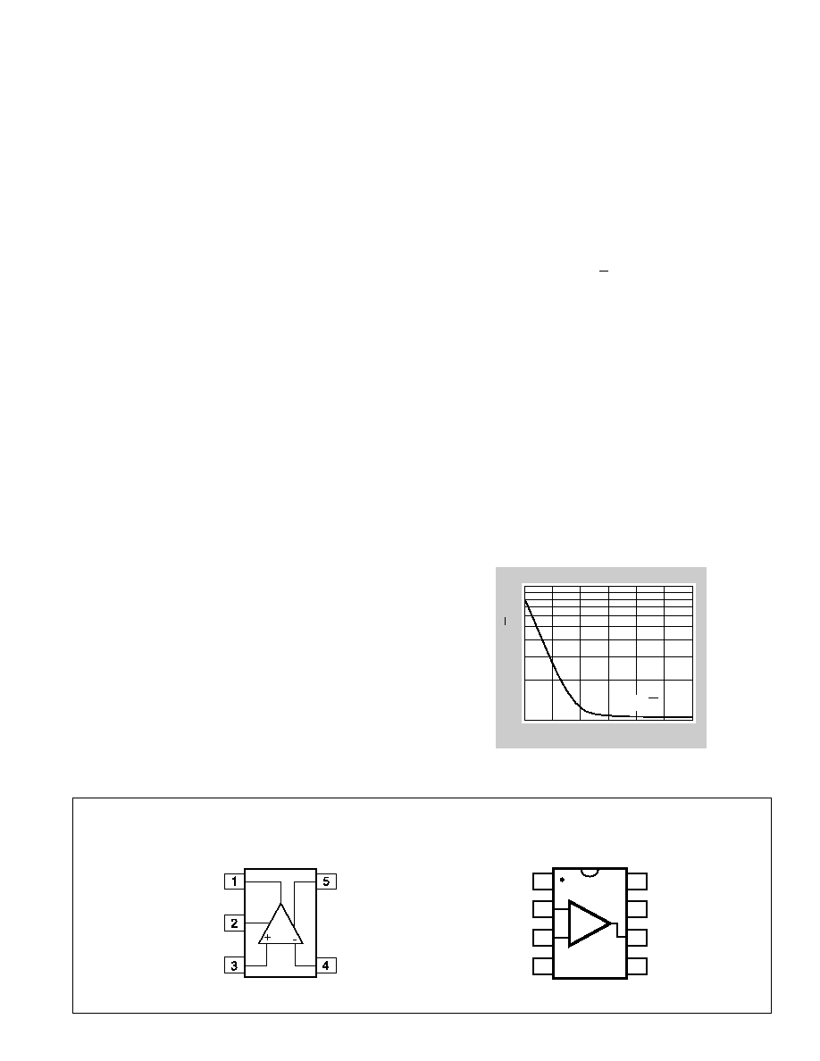
Pinout
SOT23-5
-
+
1
2
3
4
NC
V
inv
V
non-inv
-V
cc
R
p
(optional)
+V
cc
V
out
NC
8
7
6
5
Pinout
DIP & SOIC
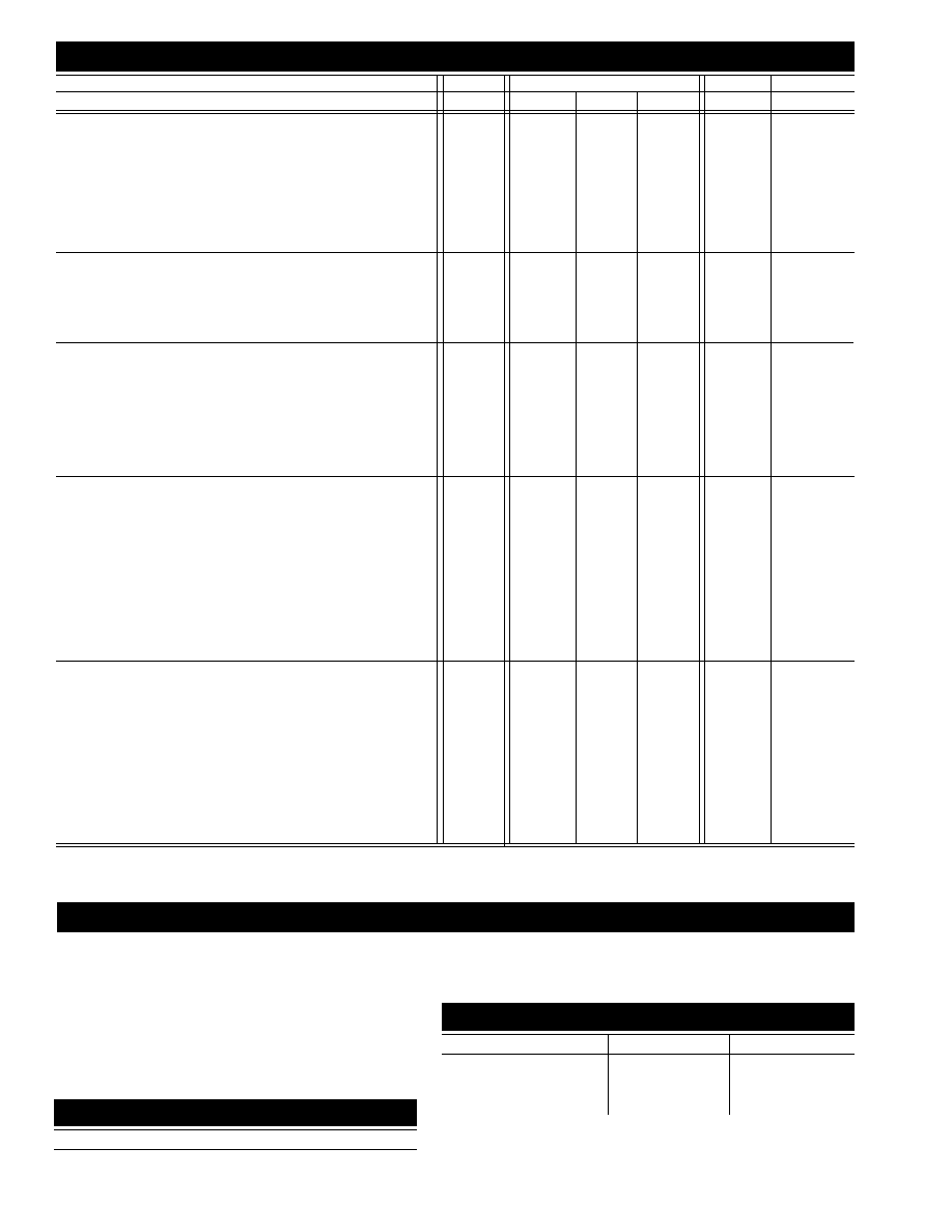
CLC425 Electrical Characteristics
(V
CC
= ±5V; A
V
= +20; R
f
=499
; R
g
= 26.1
; R
L
= 100
;
unless noted
)
PARAMETERS
CONDITIONS
TYP
MIN/MAX RATINGS
UNITS
SYMBOL
Ambient Temperature
CLC425 AJ
+25
∞
C
-40
∞
C
+25
∞
C
+85
∞
C
FREQUENCY DOMAIN RESPONSE
gain bandwidth product
V
out
< 0.4V
pp
1.9
1.5
1.5
1.0
GHz
GBW
-3dB bandwidth
V
out
< 0.4V
pp
95
75
75
50
MHz
SSBW
V
out
< 5.0V
pp
40
30
30
20
MHz
LSBW
gain flatness
V
out
< 0.4V
pp
peaking
DC to 30MHz
0.3
0.7
0.5
0.7
dB
GFP
rolloff
DC to 30MHz
0.1
0.7
0.5
0.7
dB
GFR
linear phase deviation
DC to 30MHz
0.7
1.5
1.5
2.5
∞
LPD
TIME DOMAIN RESPONSE
rise and fall time
0.4V step
3.7
4.7
4.7
7.0
ns
TRS
settling time to 0.2%
2V step
22
30
30
40
ns
TSS
overshoot
0.4V step
5
12
10
12
%
OS
slew rate
2V step
350
250
250
200
V/
µ
s
SR
DISTORTION AND NOISE RESPONSE
2
nd
harmonic distortion
1V
pp
, 10MHz
- 53
48
48
46
dBc
HD2
3
rd
harmonic distortion
1V
pp
, 10MHz
- 75
65
65
60
dBc
HD3
3
rd
order intermodulation intercept
10MHz
35
dBm
IMD
equivalent noise input
voltage
1MHz to 100MHz
1.05
1.25
1.25
1.8
nV/
Hz
VN
current
1MHz to 100MHz
1.6
4.0
2.5
2.5
pA/
Hz
ICN
noise figure
R
S
= 700
0.9
dB
NF
STATIC DC PERFORMANCE
open-loop gain
DC
96
77
86
86
dB
AOL
*input offset voltage
± 100
± 1000
± 800
± 1000
µ
V
VIO
average drift
± 2
8
____
4
µ
V/∞C
DVIO
*input bias current
12
40
20
20
µ
A
IB
average drift
- 100
- 250
____
- 120
nA/∞C
DIB
input offset current
± 0.2
3.4
2.0
2.0
µ
A
IIO
average drift
± 3
± 50
____
± 25
nA/∞C
DIIO
power supply rejection ratio
DC
95
82
88
86
dB
PSRR
common mode rejection ratio
DC
100
88
92
90
dB
CMRR
*supply current
R
L
=
15
18
16
16
mA
ICC
MISCELLANEOUS PERFORMANCE
input resistance
common-mode
2
0.6
1.6
1.6
M
RINC
differential-mode
6
1
3
3
k
RIND
input capacitance
common-mode
1.5
2
2
2
pF
CINC
differential-mode
1.9
3
3
3
pF
CIND
output resistance
closed loop
5
50
10
10
m
ROUT
output voltage range
R
L
=
± 3.8
± 3.5
± 3.7
± 3.7
V
VO
R
L
=100
± 3.4
± 2.8
± 3.2
± 3.2
V
VOL
input voltage range
common mode
± 3.8
± 3.4
± 3.5
± 3.5
V
CMIR
output current
source
80
70
70
70
mA
IOP
sink
80
45
55
55
mA
ION
Min/max ratings are based on product characterization and simulation. Individual parameters are tested as noted. Outgoing quality levels are
determined from tested parameters.
http://www.national.com
2
Absolute Maximum Ratings
Miscellaneous Ratings
V
cc
±7V
I
out
short circuit protected to ground, however maximum reliabiliy
is obtained if I
out
does not exceed...
125mA
common-mode input voltage
±V
cc
maximum junction temperature
+150
∞
C
operating temperature range:
AJ
-40∞C to +85∞C
storage temperature range
-65∞C to +150∞C
lead temperature (soldering 10 sec)
+300∞C
ESD (human body model)
1000V
Recommended gain range
±10 to ±1,000V/V
Notes:
* AJ : 100% tested at +25∞C.
Package Thermal Resistance
Package
JC
JA
AJP
70∞C/W
125∞C/W
AJE
65∞C/W
145∞C/W
A8B
45∞C/W
135∞C/W
AJM5
115∞C/W
185∞C/W
Reliability Information
Transistor count
31
3
http://www.national.com
(
µ
A)
http://www.national.com
4
Introduction
The CLC425 is a very wide gain-bandwidth, ultra-low
noise voltage feedback operational amplifier which en-
ables application areas such as medical diagnostic ultra-
sound, magnetic tape & disk storage and fiber-optics to
achieve maximum high-frequency signal-to-noise ratios.
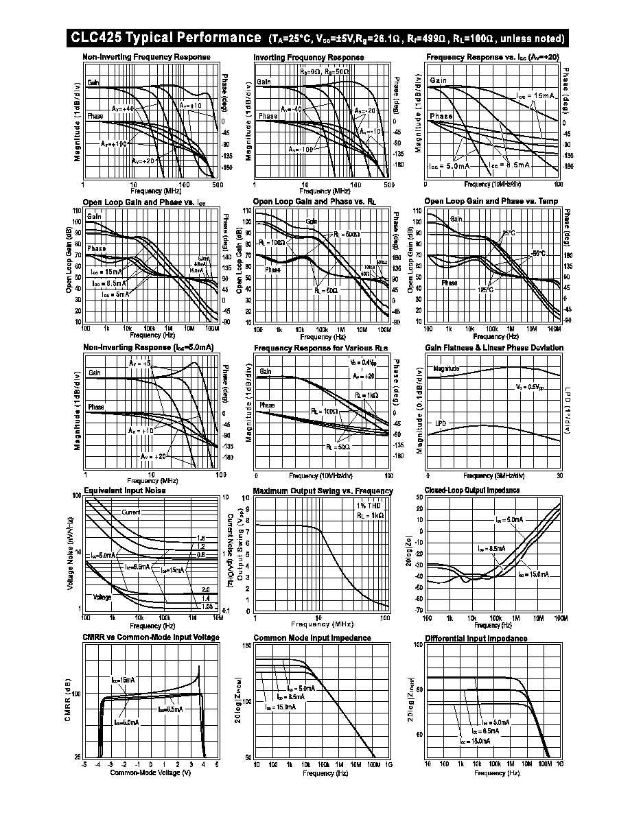
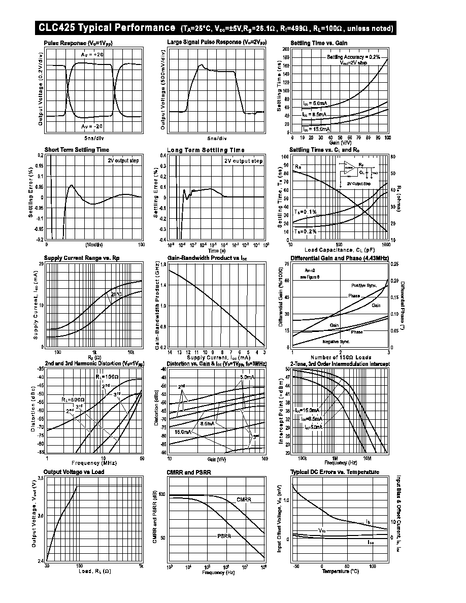
The set of characteristic plots located in the "Typical
Performance" section illustrates many of the perfor-
mance trade-offs. The following discussion will enable
the proper selection of external components in order to
achieve optimum device performance.
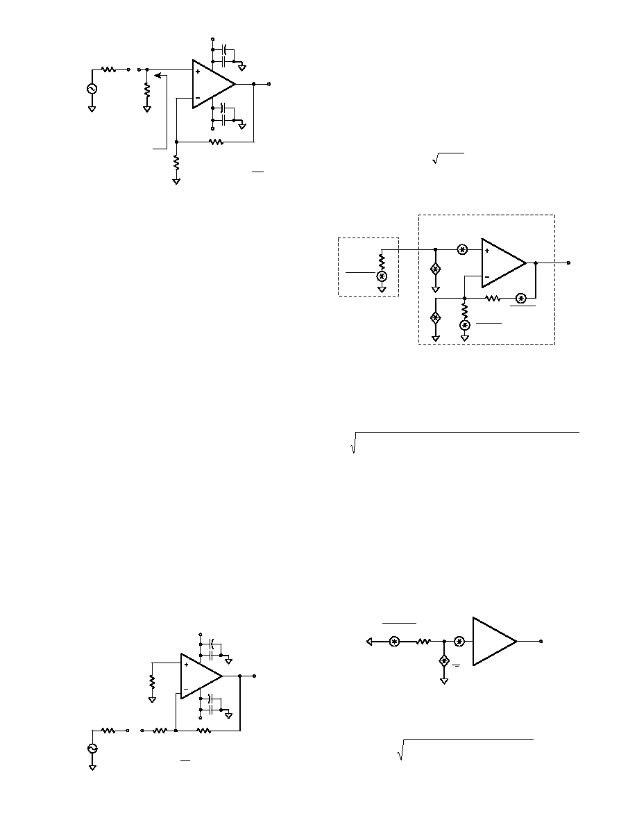
Bias Current Cancellation
In order to cancel the bias current errors of the non-
inverting configuration, the parallel combination of the
gain-setting (R
g
) and feedback (R
f
) resistors should equal
the equivalent source resistance (R
seq
) as defined in
Figure 1. Combining this constraint with the non-invert-
ing gain equation also seen in Figure 1, allows both R
f
and R
g
to be determined explicitly from the following
equations: R
f
=A
v
R
seq
and R
g
=R
f
/(A
v
-1). When driven from
a 0
source, such as that from the output of an op amp,
the non-inverting input of the CLC425 should be isolated
with at least a 25
series resistor.
As seen in Figure 2, bias current cancellation is accom-
plished for the inverting configuration by placing a resis-
tor (R
b
) on the non-inverting input equal in value to the
resistance seen by the inverting input (R
f
||(R
g
+R
s
)). R
b
is
recommended to be no less than 25
for best CLC425
performance. The additional noise contribution of R
b
can
be minimized through the use of a shunt capacitor.
4
16 4
21
25
kT
e
Joules
C
=
-
∞
.
@
R
f
3
2
4
7
6
R
g
0.1
µ
F
0.1
µ
F
6.8
µ
F
6.8
µ
F
-V
cc
+V
cc
V
out
R
T
R
s
eq
= R
s
|| R
T
R
f
R
g
A
v
= 1 +
V
s
V
in
R
s
CLC425
R
f
R
g
CLC425
R
s
eq
e
n
i
n
+
i
n
-
4kTR
g
4kTR
f
4kTR
s
eq
Total Input Noise vs. Source Resistance
In order to determine maximum signal-to-noise ratios
from the CLC425, an understanding of the interaction
between the amplifier's intrinsic noise sources and the
noise arising from its external resistors is necessary.
Figure 3 describes the noise model for the non-inverting
amplifier configuration showing all noise sources. In
addition to the intrinsic input voltage noise (e
n
) and
current noise (i
n
=i
n+
=i
n-
) sources, there also exists ther-
mal voltage noise (
e
4 TR
t
=
k
) associated with each of
the external resistors. Equation 1 provides the general
form for total equivalent input voltage noise density (e
ni
).
Equation 2 is a simplification of Equation 1 that assumes
R
f
||R
g
= R
seq
for bias current cancellation. Figure 4
illustrates the equivalent noise model using this as-
sumption. Figure 5 is a plot of e
ni
against equivalent
source resistance (R
seq
) with all of the contributing volt-
age noise sources of Equation 2 shown. This plot gives
the expected e
ni
for a given R
seq
which assumes R
f
||R
g
=
R
seq
for bias current cancellation. The total equivalent
output voltage noise (e
no
) is e
ni
A
v
.
Equation 1: General Noise Equation
e
e
i
R
kTR
i
R
R
kT R
R
ni
n
n
s
s
n
f
g
f
g
eq
eq
=
+
(
)
+
+
(
)
(
)
+
(
)
+
-
2
2
2
4
4
||
||
Figure 3: Non-inverting Amplifer Noise Model
Figure 1: Non-inverting Amplifier Configuration
Figure 4: Noise Model with R
f
||R
g
= R
seq
R
f
3
2
4
7
6
R
g
0.1
µ
F
0.1
µ
F
6.8
µ
F
6.8
µ
F
-V
cc
+V
cc
V
out
V
s
V
in
R
b
R
s
A
v
= -
R
f
R
g
CLC425
e
n
A
v
2R
s
eq
4kT2R
s
eq
i
n
2
Equation 2: Noise Equation with R
f
||R
g
= R
seq
e
e
i R
kT
R
ni
n
n
s
s
eq
eq
=
+
( )
+
( )
2
2
2
4
2
Figure 2: Inverting Amplifier Configuration
5
http://www.national.com