 | –≠–ª–µ–∫—Ç—Ä–æ–Ω–Ω—ã–π –∫–æ–º–ø–æ–Ω–µ–Ω—Ç: CLC428 | –°–∫–∞—á–∞—Ç—å:  PDF PDF  ZIP ZIP |
N
CLC428
Dual Wideband, Low-Noise, Voltage Feedback Op Amp
General Description
The CLC428 is a very high-speed dual op amp that offers a traditional
voltage-feedback topology featuring unity-gain stability and slew-
enhanced circuitry. The CLC428's ultra low noise and very low
harmonic distortion combine to form a very wide dynamic-range op
amp that operates from a single (5 to 12V) or dual (±5V) power supply.
Each of the CLC428's closely matched channels provides a 160MHz
unity-gain bandwidth with an ultra low input voltage noise density
(2nV/
Hz). Very low 2nd/3rd harmonic distortion (-62/-72dBc) as well
as high channel-to-channel isolation (-62dB) make the CLC428 a
perfect wide dynamic-range amplifier for matched I/Q channels.
With its fast and accurate settling (16ns to 0.1%), the CLC428 is also
a excellent choice for wide-dynamic range, anti-aliasing filters
to buffer the inputs of hi-resolution analog-to-digital converters.
Combining the CLC428's two tightly-matched amplifiers in a single
eight-pin SOIC reduces cost and board space for many composite
amplifier applications such as active filters, differential line drivers/
receivers, fast peak detectors and instrumentation amplifiers.
To reduce design times and assist in board layout, the CLC428 is
supported by an evaluation board and a SPICE simulation model
available from National Semiconductor.
June 1999
Features
s
Wide unity-gain bandwidth: 160MHz
s
Ultra-low noise: 2.0nV/
Hz
s
Low distortion: -78dBc 2nd (2MHz)
-62/-72dBc (10MHz)
s
Settling time: 16ns to 0.1%
s
Supply voltage range: ±2.5 to ±5 or
single supply
s
High output current: ±80mA
Applications
s
General purpose dual op amp
s
Low noise integrators
s
Low noise active filters
s
Diff-in/diff-out instrumentation amp
s
Driver/receiver for transmission systems
s
High-speed detectors
s
I/Q channel amplifiers
CLC428
Dual
Wideband,
Lo
w-Noise,
V
oltag
e
Feedbac
k Op Amp
Pinout
DIP & SOIC
1
2
3
4
8
7
6
5
V
out
1
V
inv
1
V
non-inv
1
-Vcc
+V
cc
V
out
2
V
inv
2
V
non-inv
2
-
+
-
+
Typical Application
5-Decade Integrator
©
1999 National Semiconductor
Corporation
http://www.national.com
Printed in the U.S.A.

CLC428 Electrical Characteristics
(V
CC
= ±5V; A
V
= +2V/V; R
f
=100
; R
g
=100
; R
L
= 100
; unless noted
;
PARAMETERS
CONDITIONS
TYP
MIN/MAX RATINGS
UNITS
NOTES
Ambient Temperature
CLC428
+25∞C
+25∞C
0 to +70∞C -40 to +85∞C
FREQUENCY DOMAIN RESPONSE
gain bandwidth product
V
out
< 0.5V
pp
135
100
80
70
MHz
-3dB bandwidth, Av=+1
V
out
< 0.5V
pp
160
120
90
80
MHz
Av=+2
V
out
< 0.5V
pp
80
50
40
35
MHz
V
out
< 5.0V
pp
40
25
22
20
MHz
gain flatness
V
out
< 0.5V
pp
peaking
DC to 200MHz
0.0
0.6
0.8
1.0
dB
rolloff
DC to 20MHz
0.05
0.5
0.7
0.7
dB
linear phase deviation
DC to 20MHz
0.2
1.0
1.5
1.5
∞
TIME DOMAIN RESPONSE
rise and fall time
1V step
5.5
7.5
9.0
10.0
ns
settling time
2V step to 0.1%
16
20
24
24
ns
overshoot
1V step
1
5
10
10
%
slew rate
5V step
500
300
275
250
V/
µ
s
DISTORTION AND NOISE RESPONSE
2
nd
harmonic distortion
1V
pp
,10MHz
- 62
- 50
- 45
- 43
dBc
3
rd
harmonic distortion
1V
pp
,10MHz
- 72
- 60
- 56
- 56
dBc
equivalent input noise
voltage
1MHz to 100MHz
2.0
2.5
2.8
2.8
nV/
Hz
current
1MHz to 100MHz
2.0
3.0
3.6
4.6
pA/
Hz
crosstalk
input referred, 10MHz
- 62
- 58
- 58
- 58
dB
STATIC DC PERFORMANCE
open-loop gain
60
56
50
50
dB
input offset voltage
1.0
2.0
3.0
3.5
mV
A
average drift
5
---
15
20
µ
V/
∞
C
input bias current
1.5
25
40
65
µ
A
A
average drift
150
---
600
700
nA/
∞
C
input offset current
0.3
3
5
5
µ
A
average drift
5
---
25
50
nA/
∞
C
power supply rejection ratio
66
60
55
55
dB
common-mode rejection ratio
63
57
52
52
dB
supply current
per channel, R
L
=
11
12
13
15
mA
A
MISCELLANEOUS PERFORMANCE
input resistance
common-mode
500
250
125
125
k
differential-mode
200
50
25
25
k
input capacitance
common-mode
2.0
3.0
3.0
3.0
pF
differential-mode
2.0
3.0
3.0
3.0
pF
output resistance
closed loop
0.05
0.1
0.2
0.2
output voltage range
R
L
=
± 3.8
± 3.5
± 3.3
± 3.3
V
R
L
=100
± 3.5
± 3.2
± 2.6
± 1.3
V
input voltage range
common mode
± 3.7
± 3.5
± 3.3
± 3.3
V
output current
± 70
± 50
± 40
± 20
mA
Min/max ratings are based on product characterization and simulation. Individual parameters are tested as noted. Outgoing quality levels are
determined from tested parameters.
Ordering Information
supply voltage
±7V
short circuit current
(note 1)
common-mode input voltage
±V
cc
differential input voltage
±10V
maximum junction temperature
+150
∞
C
storage temperature
-65∞C to+150∞C
lead temperature (soldering 10 sec)
+300∞C
Absolute Maximum Ratings
Model
Temperature Range
Description
CLC428AJP
-40∞C to +85∞C
8-pin PDIP
CLC428AJE
-40∞C to +85∞C
8-pin SOIC
CLC428A8B
-55∞C to +125∞C
8-pin CerDIP, MIL-STD-883
DESC SMD number: 5962-94708
http://www.national.com
2
Package
jc
jA
Plastic (AJP)
60∞C/W
115∞C/W
Surface Mount (AJE)
40∞C/W
115∞C/W
CerDIP
25∞C/W
115∞C/W
Package Thermal Resistance
Notes
A) J-level: spec is 100% tested at +25∞C, sample tested at +85∞C.
1) Output is short circuit protected to ground, however maximum
reliability is obtained if output current does not exceed 160mA.
Transistor count
104
Reliability Information
3
http://www.national.com

Application Discussion
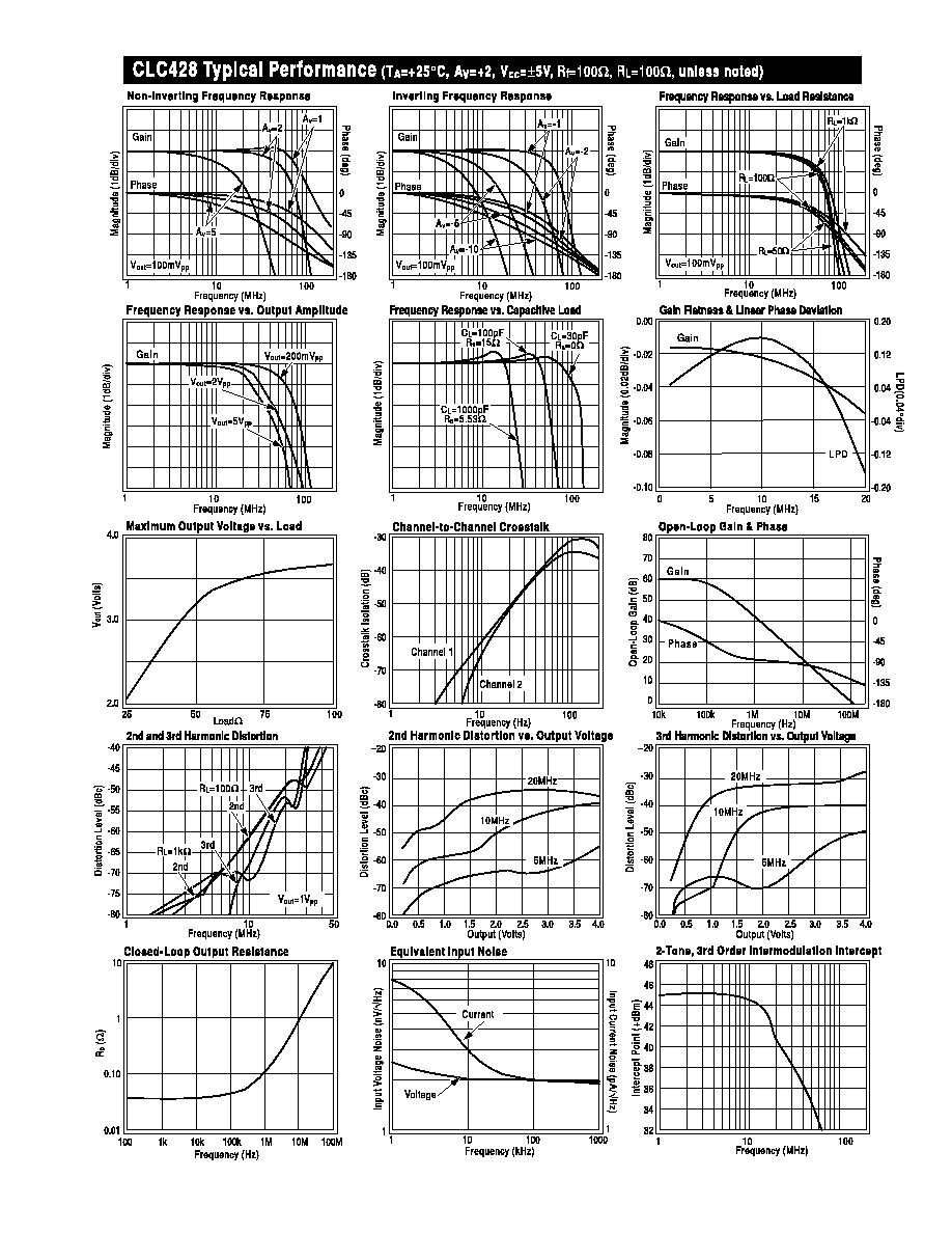
Low Noise Design
Ultimate low noise performance from circuit designs using
the CLC428 requires the proper selection of
external resistors. By selecting appropriate low-valued
resistors for R
f
and R
g
, amplifier circuits using the CLC428
can achieve output noise that is approximately the
equivalent voltage input noise of 2.0 nV/
Hz multiplied
by the desired gain (Av).
Each amplifier in the CLC428 has an equivalent
input noise resistance which is optimum for matching
source impedances of approximately 1k. Using a
transformer, any source can be matched to achieve the
lowest noise design.
For even lower noise performance than the CLC428,
consider the CLC425 or CLC426 at 1.05 and 1.6 nV/
Hz,
respectively.
DC Bias Currents and Offset Voltages
Cancellation of the output offset voltage due to input bias
currents is possible with the CLC428. This is done by
making the resistance seen from the inverting and non-
inverting inputs equal. Once done, the residual output
offset voltage will be the input offset voltage (Vos) multi-
plied by the desired gain (Av). Comlinear Application Note
OA-7 offers several solutions to further reduce the output
offset.
Output and Supply Considerations
With ±5V supplies, the CLC428 is capable of a typical
output swing of ±3.8V under a no-load condition.
Additional output swing is possible with slightly higher
supply voltages. For loads of less than 50
, the output
swing will be limited by the CLC428's output current
capability, typically 80mA.
Output settling time when driving capacitive loads can be
improved by the use of a series output resistor. See the
plot labeled "Settling Time vs. Capacitive Load" in the
Typical Performance section.
Layout
Proper power supply bypassing is critical to insure good high
frequency performance and low noise. De-coupling capaci-
tors of 0.1
µ
F should be place as close as possible to the
power supply pins. The use of surface mounted capacitors
is recommended due to their low series inductance.
A good high frequency layout will keep power supply and
ground traces away from the inverting input and output
pins. Parasitic capacitance from these nodes to ground
causes frequency response peaking and possible circuit
oscillation. See OA-15 for more information. National
suggests the CLC730038 (through-hole) or the CLC730036
(SOIC) dual op amp evaluation board as a guide for high
frequency layout and as an aid in device evaluation.
http://www.national.com
4
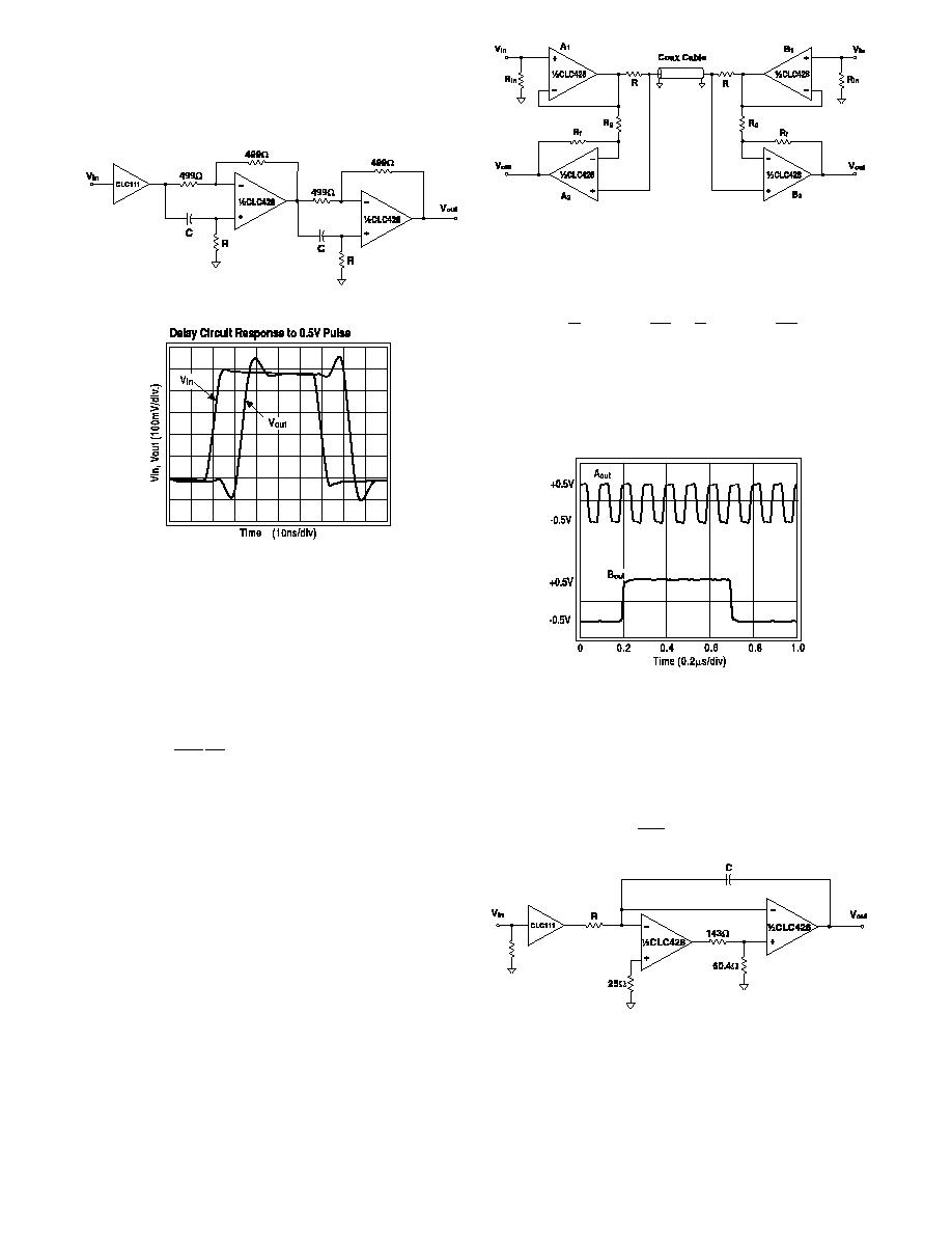
Analog Delay Circuit (All-Pass Network)
The circuit in Figure 1 implements an all-pass network using
the CLC428. A wide bandwidth buffer (CLC111) drives the
circuit and provides a high input impedence for the source.
As shown in Figure 2, the circuit provides a
Figure 1
Figure 2
13.1ns delay (with R =40.2
, C=47pF). R
f
and R
g
should
be of equal and low value for parasitic insensitive opera-
tion. The circuit gain is +1 and the delay is determined by
the following equations.
delay
d
RC
T
=
+
2 2
c
h
Eq. 1
T
d
df
d
=
1
360
;
Eq. 2
where T
d
is the delay of the op amp at A
V
=+1. The CLC428
provides a typical delay of 2.8ns at its -3dB point.
Full Duplex Digital or Analog Transmission
Simultaneous transmission and reception of analog or
digital signals over a single coaxial cable or twisted-pair
line can reduce cabling requirements. The CLC428's wide
bandwidth and high common-mode rejection in a differen-
tial amplifier configuration allows full duplex transmission
of video, telephone, control and audio signals.
In the circuit shown in Figure 3, one of the CLC428's amps
is used as a "driver" and the other as a difference
"receiver" amplifier. The output impedance of the "driver"
is essentially zero. The two R's are chosen to match the
characteristic impedance of the transmission line. The
"driver" op amp gain can be selected for unity or greater.
Receiver amplifier A
2
(B
2
) is connected across R and
forms differential amplifier for the signals transmitted by
driver A
1
(B
1
). If the coax cable is lossless and R
f
equals
R
g
, receiver A
2
(B
2
) will then reject the signals from driver
Figure 3
A
1
(B
1
) and pass the signals from driver B
1
(A
1
). The
output of the receiver amplifier will be:
V
V
R
R
V
R
R
out
in
f
g
in
f
g
A B
A B
B A
e j
a f
a f
=
-
F
H
G
G
I
K
J
J
+
+
F
H
G
G
I
K
J
J
1
2
1
1
2
1
Eq. 3
Care must be given to layout and component placement to
maintain a high frequency common-mode rejection. The
plot of Figure 4 shows the simultaneous reception of
signals transmitted at 1MHz and 10MHz.
Figure 4
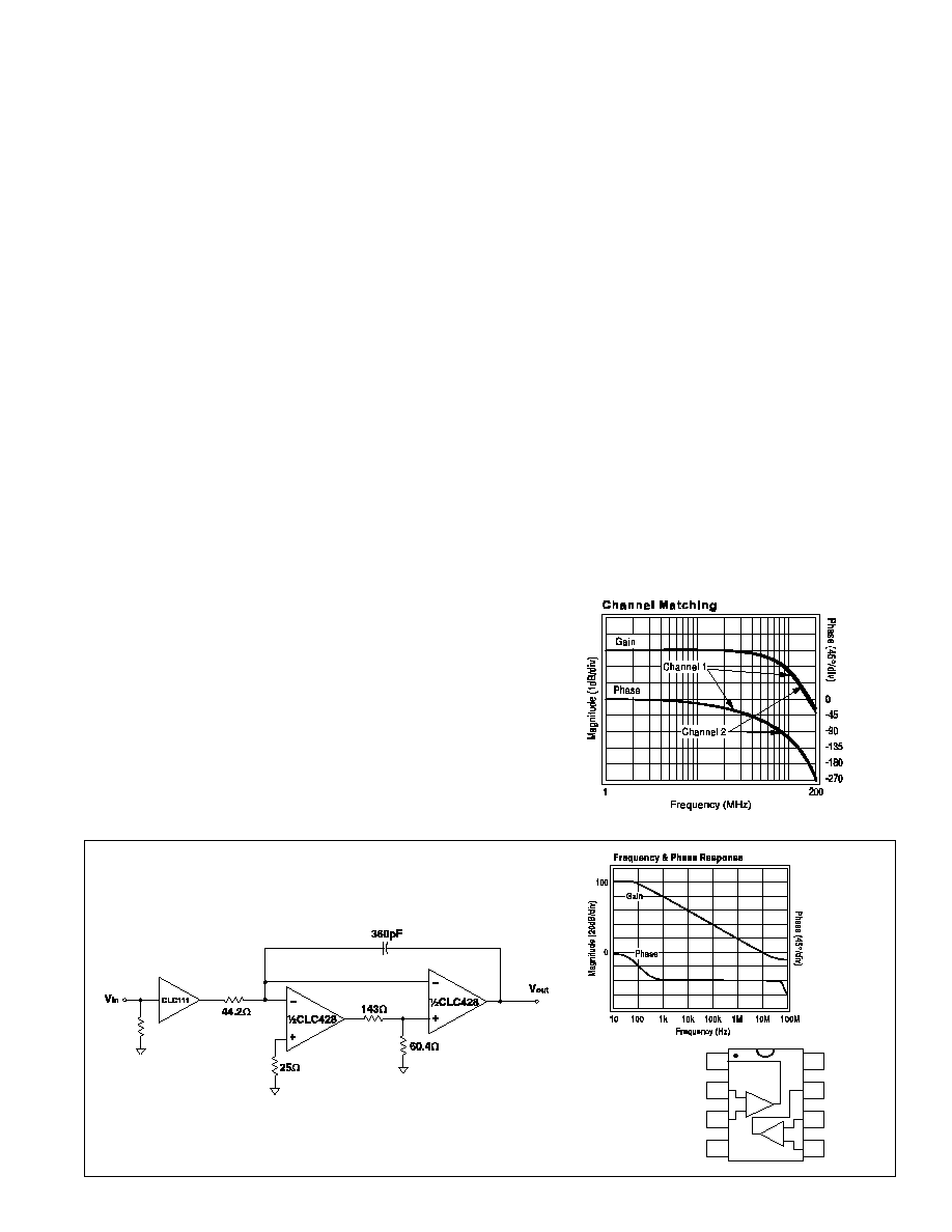
Five Decade Integrator
A composite integrator, as shown in Figure 5, uses the
CLC428 dual op amp to increase the circuits' usable
frequency range of operation. The transfer function of this
circuit is:
V
1
RC
V dt
o
in
=
z
Eq. 4
Figure 5
A resistive divider made from the 143
and 60.4
resistors was chosen to reduce the loop-gain and stabilize
the network. The CLC428 composite integrator provides
integration over five decades of operation. R and C set the
integrator's gain. Figure 6 shows the frequency and phase
response of the circuit in Figure 5 with R = 44.2
and
C = 360pF.
5
http://www.national.com