 | –≠–ª–µ–∫—Ç—Ä–æ–Ω–Ω—ã–π –∫–æ–º–ø–æ–Ω–µ–Ω—Ç: CLC432 | –°–∫–∞—á–∞—Ç—å:  PDF PDF  ZIP ZIP |
N
CLC431/432
Dual Wideband Monolithic Op Amp with Disable
General Description
The CLC431 and CLC432 current-feedback amplifiers provide wide
bandwidths and high slew rates for applications where board density
and power are key considerations. These amplifiers provide DC-
coupled small signal bandwidths exceeding 92MHz while consuming
only 7mA per channel. Operating from ±15V supplies, the CLC431/
432's enhanced slew rate circuitry delivers large-signal bandwidths
with output voltage swings up to 28V
pp
. A wide range of bandwidth-
insensitive gains are made possible by virtue of the CLC431 and
CLC432's current-feedback topology.
The large common-mode input range and fast settling time (70ns
to 0.05%) make these amplifiers well suited for CCD & data
telecommunication applications. The disable of the CLC431 can
accommodate ECL or TTL logic levels or a wide range of user
definable inputs. With its fast enable/disable time (0.2
µ
s/1
µ
s) and
high channel isolation of 70dB at 10MHz, the CLC431 can easily be
configured as a 2:1 MUX. Many high performance video applications
requiring signal gain and/or switching will be satisfied with the
CLC431/432 due to their very low differential gain and phase errors
(less than 0.1% and 0.1∞; A
v
= +2V/V at 4.43MHz into 150
load).
Quick 8ns rise and fall times on 10V pulses allow the CLC431/432 to
drive either twisted pair or coaxial transmission lines over long
distances.
The CLC431/432's combination of low input voltage noise, wide
common-mode input voltage range and large output voltage swings
make them especially well suited for wide dynamic range signal
processing applications.
June 1999
CLC431/432
Dual
Wideband Monolithic Op Amp with Disab
le
Features
s
Wide bandwidth: 92MHz (A
V
=+1)
62MHz (A
v
=+2)
s
Fast slew rate: 2000V/
µ
s
s
Fast disable: 1
µ
s to high-Z output
s
High channel isolation: 70dB at 10MHz
s
Single or dual supplies: ±5V to ±16.5V
Applications
s
Video signal multiplexing
s
Twisted-pair differential driver
s
CCD buffer & level shifting
s
Discrete gain-select amplifier
s
Transimpedance amplifier
©
1999 National Semiconductor Corporation
http://www.national.com
Printed in the U.S.A.
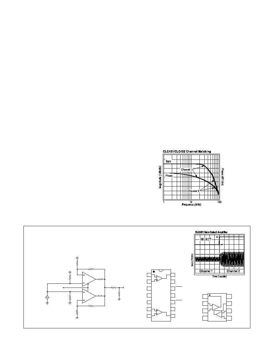
1V
pp
@ 5MHz
R
f
Channel 1 (Gain = 2)
Channel 2 (Gain = 5)
R
f
R
i
R
i
R
s
R
L
R
g
R
g
V
out
SELECT
ΩCLC431
ΩCLC431
50
50
50
50
50
50
500
500
500
125
Typical Application
Discrete Gain Select Amplifier
-
+
-
+
1
2
3
4
V
out
1
V
inv
1
V
non-inv
1
-Vcc
+V
cc
V
out
2
V
inv
2
V
non-inv
2
8
7
6
5
V
inv
1
V
non-inv
1
DIS1
-V
cc
DIS2
V
non-inv
2
V
inv
2
V
out
1
V
R
TTL
1
DIS1
+V
cc
DIS2
V
R
TTL
2
V
out
2
1
2
3
4
5
6
7
14
13
12
11
10
9
8
CLC432
CLC431
Pinout
PDIP & SOIC
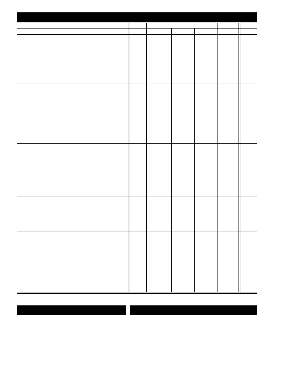
CLC431/432 Electrical Characteristics
(V
CC
= ±15V; A
V
= +2; R
f
= R
g
=750
; R
L
= 100
; unless noted)
http://www.national.com
2
supply voltage
±16.5V
short circuit current
100mA
common-mode input voltage
±V
cc
differential input voltage
±10V
maximum junction temperature
+150
∞
C
storage temperature
-65∞C to+150∞C
lead temperature (soldering 10 sec)
+300∞C
1) Tested and guaranteed with R
f
= 866
.
CLC432 tested and guaranteed
with R
f
= 750
.
2) Spec is guaranteed for R
L
500
.
3) V
RTTL
= 0, See text for single-ended mode of operation.
4) V
RTTL
= NC, See text for differential mode of operation
5) Spec is guaranteed for AJE; AJP & AIB yield 7dB lower.
6) Spec is tested with 2V
pp
, 10MHz and R
L
= 100
.
A) J-level: spec is 100% tested at +25∞C.
Absolute Maximum Ratings
Notes
PARAMETERS
CONDITIONS
TYP
MIN/MAX RATINGS
UNITS
NOTES
Ambient Temperature
CLC431 & CLC432
+25
+25
0 to +70
-40 to +85
∞C
1
FREQUENCY DOMAIN RESPONSE
-3dB bandwidth
V
out
< 4.0V
pp
62
42
37
36
MHz
V
CC
= ±5V
V
out
< 4.0V
pp
62
MHz
V
out
< 10V
pp
28
21
20
20
MHz
2
gain flatness
V
out
< 4.0V
pp
peaking
DC to 100MHz
0.05
0.5
0.7
0.7
dB
rolloff
DC to 20MHz
0.0
0.8
0.8
0.8
dB
linear phase deviation
DC to 30MHz
0.3
1.8
2.0
2.1
∞
differential gain
4.43MHz, R
L
=150
0.12
0.18
0.2
0.2
%
differential phase
4.43MHz, R
L
=150
0.12
0.18
0.23
0.25
∞
TIME DOMAIN RESPONSE
rise and fall time
10V step
8
12
13
13
ns
2
overshoot
2V step
5
10
12
12
%
settling time
2V step to 0.05%
70
100
110
110
ns
slew rate
V
out
= ±10V
2000
1500
1450
1400
V/ms
2
DISTORTION AND NOISE RESPONSE
2
nd
harmonic distortion
2V
pp
, 1MHz
- 65
dBc
6
3
rd
harmonic distortion
2V
pp
, 1MHz
- 75
dBc
6
equivalent input noise
voltage
>1MHz
3.3
4.2
4.4
4.5
nV/
Hz
current, inverting
>1MHz
13
16
17
18
pA/
Hz
current, non-inverting
>1MHz
2.0
2.5
2.6
2.8
pA/
Hz
STATIC DC PERFORMANCE
input
offset voltage
3
6
7
7
mV
A
average drift
20
---
50
50
µ
V/∞C
bias current, non-inverting
2
8
10
16
µ
A
A
average drift
25
---
100
150
nA/∞C
bias current, inverting
2
6
6
8
µ
A
A
average drift
8
---
25
40
nA/∞C
power supply rejection ratio
DC
64
59
59
59
dB
common-mode rejection ratio
DC
63
58
57
56
dB
supply current
R
L
=
, per channel
7.1
7.9
8.5
9.6
mA
A
CLC431 disabled
R
L
=
, per channel
0.8
1.2
1.3
1.45
mA
A
MISCELLANEOUS PERFORMANCE
input
voltage range
common mode
± 12.2
± 12.0
± 11.8
± 11.6
V
resistance
non-inverting
24
16
10
6
M
capacitance
non-inverting
0.5
1
1
1
pF
output
current
± 60
± 38
± 35
± 30
mA
voltage range
R
L
5k
± 14.0
± 13.6
± 13.4
± 13.2
V
R
L
=100
± 6.0
± 3.7
± 3.7
± 2.9
V
SWITCHING PERFORMANCE (CLC431)
switching time
turn on
0.1
0.15
0.155
0.165
µ
s
turn off
0.7
1.0
1.2
1.2
µ
s
DIS logic levels
single-ended mode
3
high input voltage (V
IH
)
> 2.0
> 2.0
> 2.0
> 2.0
V
low input voltage (V
IL
)
< 0.8
< 0.8
< 0.8
< 0.8
V
maximum current input
V
IH
> DIS > V
IL
150
180
190
205
µ
A
|DIS-DIS|
differential mode
4
minimum differential voltage
0.3
0.4
0.4
0.4
V
ISOLATION
crosstalk, input referred
10MHz
70
64
64
64
dB
off isolation
10MHz
64
60
60
60
dB
5
Min/max ratings are based on product characterization and simulation. Individual parameters are tested as noted. Outgoing quality levels are
determined from tested parameters.
3
http://www.national.com
http://www.national.com
4
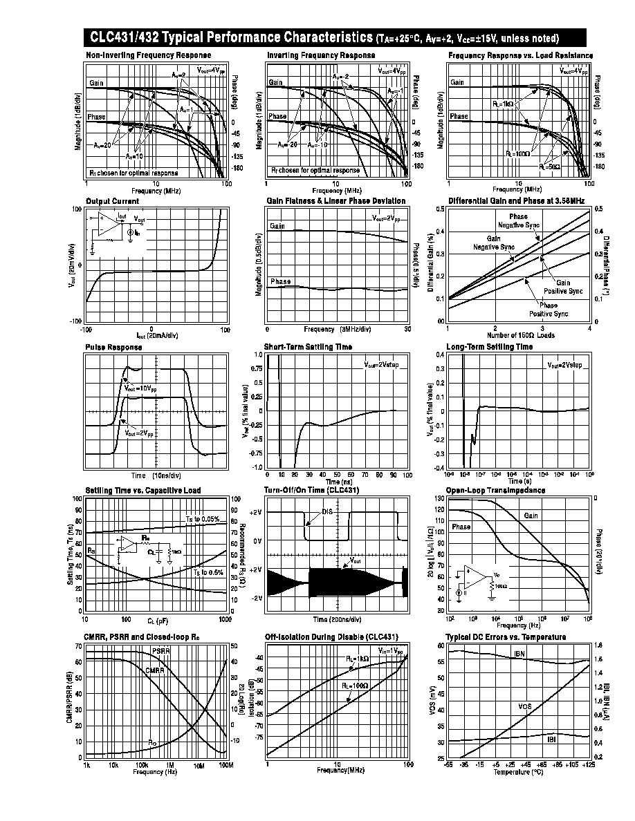
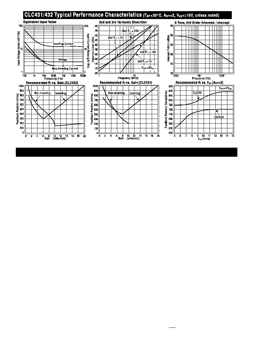
Typical Performance plots are valid for both devices
under the specified conditions. Generally, lowering R
f
from its recommended value will peak the frequency
response and extend the bandwidth while increasing its
value will roll off the response. Reducing the value of R
f
too far below its recommended value will cause overshoot,
ringing and eventually oscillation. For more information
see Application Note OA-20 and OA-13.
In order to optimize the devices' frequency and phase
response for gains other than +2V/V it is recommended
to adjust the value of the feedback resistor. The two plots
found in the Typical Performance section entitled
"Recommended R
f
vs. Gain" provide the means of
selecting the feedback-resistor value that optimizes
frequency and phase response over the CLC431/
CLC432's gain range. Both plots show the value of R
f
approaching a nonzero minimum at high non-inverting
gains, which is characteristic of current-feedback op
amps and yields best results. The linear portion of the
two R
f
vs. Inverting-gain curves results from the limitation
placed on R
g
(i.e. R
g
50
) in order to maintain an
adequate input impedance for the inverting configuration.
It should be noted that for stable operation a non-
inverting gain of +1 requires an R
f
equal to 1k
for both
the CLC431 and the CLC432.
CLC431 Disable Feature
The CLC431 disable feature can be operated either
single-endedly or differentially thereby accommodating a
wide range of logic families. There are three pins asso-
ciated with the disable feature of each of the CLC431's
two amplifiers:
DIS DIS and V
RTTL
,
(please see pinout on
Introduction
The CLC431 and the CLC432 are dual wideband current-
feedback op amps that operate from single (+10V to
+33V) or dual (±5V to ±16.5) power supplies. The
CLC431 is equipped with a disable feature and is offered
in 14-pin DIP and SOIC packages. The CLC432 is
packaged in a standard 8-pin dual pinout and is offered
in an 8-pin DIP and SOIC. Evaluation boards are available
for each version of both devices. The evaluation boards
can assist in the device and/or application evaluation and
were used to generate the typical device performance
plots on the preceding pages.
Each of the CLC431/CLC432's dual channels provide
closely matched DC & AC electrical performance
characteristics making them ideal choices for wideband
signal processing. The CLC431, with its disable feature,
can easily be configured as a 2:1 mux or several can be
used to form a 10:1 mux without performance degradation.
The two closely-matched channels of the CLC432 can be
combined to form composite circuits for such applications
as filter blocks, integrators, transimpedance amplifiers
and differential line drivers and receivers.
Feedback Resistor Selection
The loop gain and frequency response for a current-
feedback operational amplifier is determined largely by
the feedback resistor (R
f
). Package parasitics also
influence ac response. Since the package parasitics of
the CLC431 and the CLC432 are different, the optimum
frequency and phase responses are obtained with different
values of feedback resistor (for A
V
=+2; CLC431: R
f
=866
,
CLC432: R
f
=750
). The Electrical Characteristics and
Application Discussion
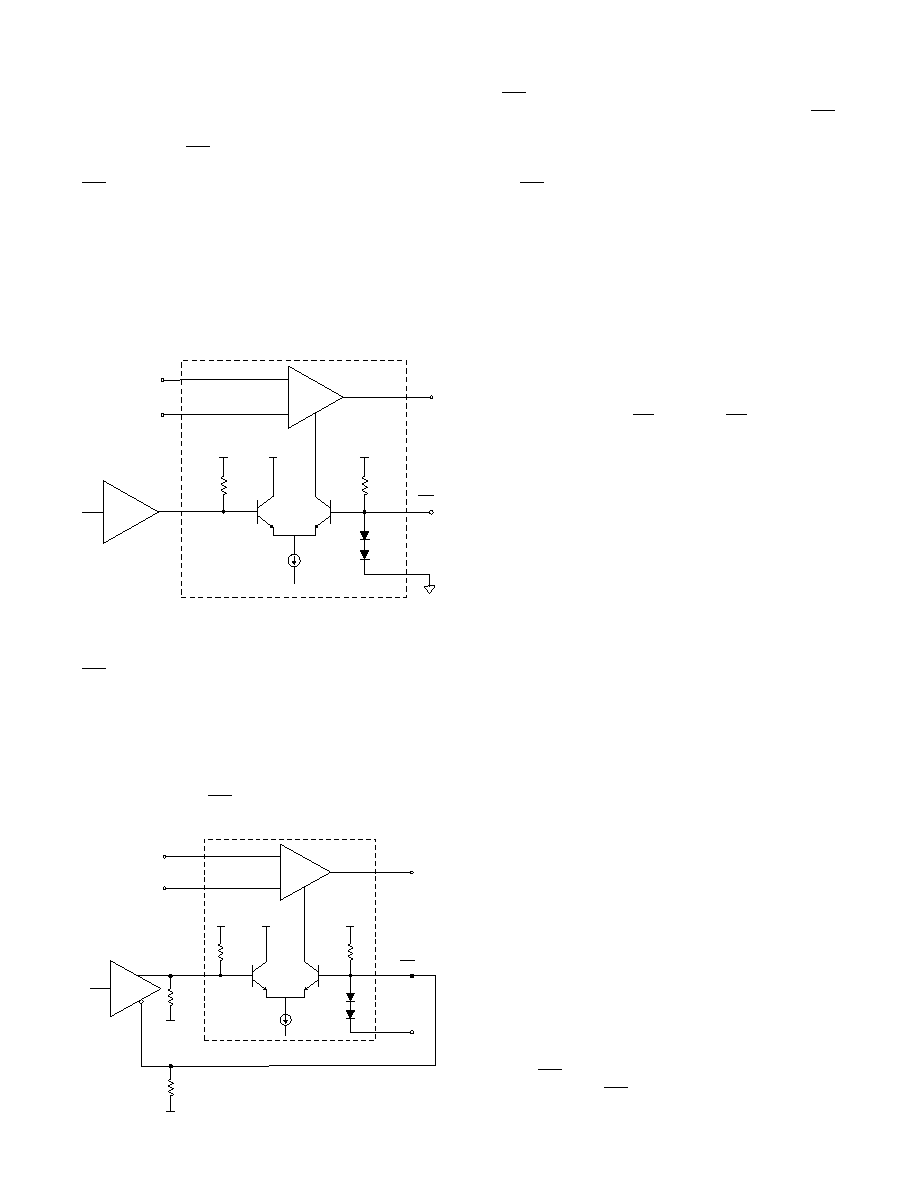
Fig. 2 illustrates the differential mode of the CLC431's
disable feature for ECL-type logic. In order for this mode
to operate properly,
V
RTTL
must be left floating while DIS
and
DIS
are to be connected directly to the ECL gate as
illustrated. Applying a differential logic "high" (DIS -
DIS
0.4Volts) switches the tail current of the differential pair
from Q2 to Q1 and results in the
disabling of that CLC431
channel. Alternatively, applying a differential logic "low"
(DIS -
DIS
-0.4Volts) switches the tail current of the
differential pair from Q1 to Q2 and results in the
enabling
of that same channel. The internal clamp, mentioned
above, also protects against excessive differential volt-
ages up to 30Volts while limiting input currents to <3mA.
DC Performance
A current-feedback amplifier's input stage does not have
equal nor correlated bias currents, therefore they cannot
be cancelled and each contributes to the total DC offset
voltage at the output by the following equation:
The input resistor R
s
is that resistance seen when looking
from the non-inverting input back towards the source. For
inverting DC-offset calculations, the source resistance
seen by the input resistor R
g
must be included in the
output offset calculation as a part of the non-inverting
gain equation. Application note OA-7 gives several circuits
for DC offset correction.
Layout Considerations
It is recommended that the decoupling capacitors (0.1
µ
F
ceramic and 6.8
µ
F electrolytic) should be placed as close
as possible to the power supply pins to insure a proper
high-frequency low impedance bypass. Careful attention
to circuit board layout is also necessary for best
performance. Of particular importance is the control of
parasitic capacitances (to ground) at the output and
invering input pins. See CLC431/432 Evaluation Board
literature for more information.
Applications Circuits
2:1 Video Mux (CLC431)
Fig. 3 illustrates the connections necessary to configure
the CLC431 as a 2:1 multiplexer in a 75
system. Each
of the two CLC431's amplifiers is configured with a non-
inverting gain of +2V/V using 634
feedback (R
f
) and
gain-setting (R
g
) resistors. The feedback resistor value is
lower than that recommended in order to compensate for
the reduction of loop-gain that results from the inclusion
of the 50
resistor (R
i
) in the feedback loop. This 50
resistor serves to isolate the output of the active channel
from the impedance of the inactive channel yet does not
affect the low output impedance of the active channel.
Notice that for proper operation
V
RTTL
1
(pin 13) is grounded
and
V
RTTL
2
(pin 9) is unconnected. The pins associated
with the disable feature are to be connected as follows:
DIS1 and
DIS2
(pins 3 & 10) are connected together as
well as
DIS2 and
DIS1
(pins 5 & 12). Channel 1 is
selected with the application of a logic "low" to SELECT
while a logic "high" selects Channel 2.
front page). Also note that both amplifiers are guaranteed
to be enabled if all three of these pins are unconnected.
Fig. 1 illustrates the single-ended mode of the CLC431's
disable feature for logic families such as TTL and CMOS.
In order to operate properly,
V
RTTL
must be grounded,
thereby biasing
DIS
to approximately +1.4V through the
two internal series diodes. For single-ended operation,
DIS
should be left floating. Applying a TTL or CMOS logic
"high" (i.e. >2.0Volts) to DIS will switch the tail current of
the differential pair to Q1 and "shut down" Q2 which
results in the
disabling of that channel of the CLC431.
Alternatively, applying a logic "low" (i.e. <0.8Volts) to DIS
will switch the tail current from Q1 to Q2 effectively
enabling that channel. If DIS is left floating under single-
ended operation, then the associated amplifier is guaran-
teed to be
disabled.
The disable feature of the CLC431 is such that DIS and
DIS
have common-mode input voltage ranges of (+V
CC
)
to (-V
CC
+3V) and are so guaranteed over the commercial
temperature range. Internal clamps (not shown) protect
the DIS input from excessive input voltages that could
otherwise cause damage to the device. This condition
occurs when enough source current flows into the node
so as to allow DIS to rise to V
CC
. This clamp is activated
once DIS exceeds
DIS
by 1.5Volts and guarantees that
V
DIS
(ground referenced) does not exceed 4.7Volts.
V
RTTL
+V
CC
+V
CC
+V
CC
DIS
DIS
V
non-inv
V
inv
V
out
ΩCLC431
100k
100k
Q
1
Q
2
TTL
CMOS
+
-
Fig. 1
V
I
R
R
R
V
R
R
I
R
offset
bn
s
f
g
io
f
g
bi
f
= ±
+
+
+
+
1
1
5
http://www.national.com
V
RTTL
+V
CC
+V
CC
+V
CC
DIS
DIS
100k
100k
Q
1
Q
2
ECL
510
-5V
-5V
510
V
non-inv
V
inv
V
out
ΩCLC431
+
-
Fig. 2