 | –≠–ª–µ–∫—Ç—Ä–æ–Ω–Ω—ã–π –∫–æ–º–ø–æ–Ω–µ–Ω—Ç: CLC432AJE | –°–∫–∞—á–∞—Ç—å:  PDF PDF  ZIP ZIP |

CLC431/432
Dual Wideband Monolithic Op Amp with Disable
General Description
The CLC431 and CLC432 current-feedback amplifiers
provide wide bandwidths and high slew rates for applications
where board density and power are key considerations.
These
amplifiers
provide
DC-coupled
small
signal
bandwidths exceeding 92MHz while consuming only 7mA
per
channel.
Operating
from
±
15V
supplies,
the
CLC431/432's
enhanced
slew
rate
circuitry
delivers
large-signal bandwidths without out voltage swings up to
28V
pp
. A wide range of bandwidth insensitive gains are
made possible by virtue of the CLC431 and CLC432's
current-feedback topology.
The large common-mode input range and fast settling time
(70ns to 0.05%) make these amplifiers well suited for CCD &
data telecommunication applications. The disable of the
CLC431 can accommodate ECL or TTL logic levels or a wide
range of user definable inputs. With its fast enable/disable
time (0.2µs/1µs) and high channel isolation of 70dB at
10MHz, the CLC431 can easily be configured as a 2:1 MUX.
Many high performance video applications requiring signal
gain and/or switching will be satisfied with the CLC431/432
due to their very low differential gain and phase errors (less
than 0.1% and 0.1∞; A
V
= +2V/V at 4.43MHz into 150
load).
Quick 8ns rise and fall times on 10V pulses allow the
CLC431/432
to
drive
either
twisted
pair
or
coaxial
transmission lines over long distances.
The CLC431/432's combination of low input voltage noise,
wide common-mode input voltage range and large output
voltage swings make them especially well suited for wide
dynamic range signal processing applications
Enhanced Solutions (Military/Aerospace)
SMD Number: 5962-94725
*
Space level versions also available.
*
For more information, visit http://www.national.com/mil
Features
n
Wide bandwidth:
92MHz(A
V
=+1), 62MHz(A
V
=+2)
n
Fast slew rate: 2000V/µs
n
Fast disable: 1µs to high-Z output
n
High channel isolation: 70dB at 10MHz
n
Single or dual supplies:
±
5V to
±
16.5V
Applications
n
Video signal multiplexing
n
Twisted-pair differential driver
n
CCD buffer & level shifting
n
Discrete gain-select amplifier
n
Transimpedance amplifier
Connection Diagrams
CLC431/CLC432 Channel Matching
DS012712-1
DS012712-5
Pinout
CLC432 DIP & SOIC
February 2001
CLC431/432
Dual
W
ideband
Monolithic
Op
Amp
with
Disable
© 2001 National Semiconductor Corporation
DS012712
www.national.com
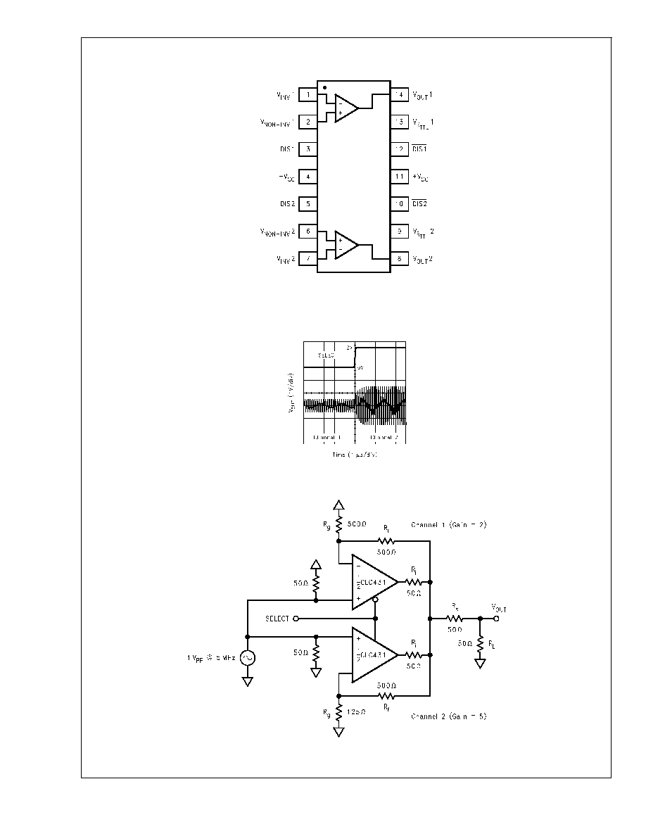
Connection Diagrams
(Continued)
Typical Application
DS012712-4
Pinout
CLC431 DIP & SOIC
DS012712-3
CLC431 Gain-Select Amplifier
DS012712-2
Discrete Gain-Select Amplifier
CLC431/432
www.national.com
2

Ordering Information
Package
Temperature Range
Industrial
Part Number
Package
Marking
NSC
Drawing
14-Pin Plastic DIP
-40∞C to +85∞C
CLC431AJP
CLC431AJP
N14A
14-Pin Plastic SOIC
-40∞C to +85∞C
CLC431AJE
CLC431AJE
M14A,B
8-Pin Plastic DIP
-40∞C to +85∞C
CLC432AJP
CLC432AJP
N08E
8-Pin Plastic SOIC
-40∞C to +85∞C
CLC432AJE
CLC432AJE
M08A
CLC431/432
www.national.com
3
Absolute Maximum Ratings
(Note 1)
If Military/Aerospace specified devices are required,
please contact the National Semiconductor Sales
Office/Distributors for availability and specifications.
Supply Voltage
±
16.5V
Short Circuit Current
100mA
Common-Mode Input Voltage
±
V
CC
Differential Input voltage
±
10V
Maximum Junction Temperature
150∞C
Storage Temperature Range
-65∞C to +150∞C
Lead Temperature (Soldering 10 sec)
+300∞C
Operating Ratings
Thermal Resistance
Package
(
JC
)
(
JA
)
14-Pin MDIP
55∞C/W
100∞C/W
14-Pin SOIC
35∞C/W
105∞C/W
8-Pin MDIP
55∞C/W
110∞C/W
8-Pin SOIC
40∞C/W
115∞C/W
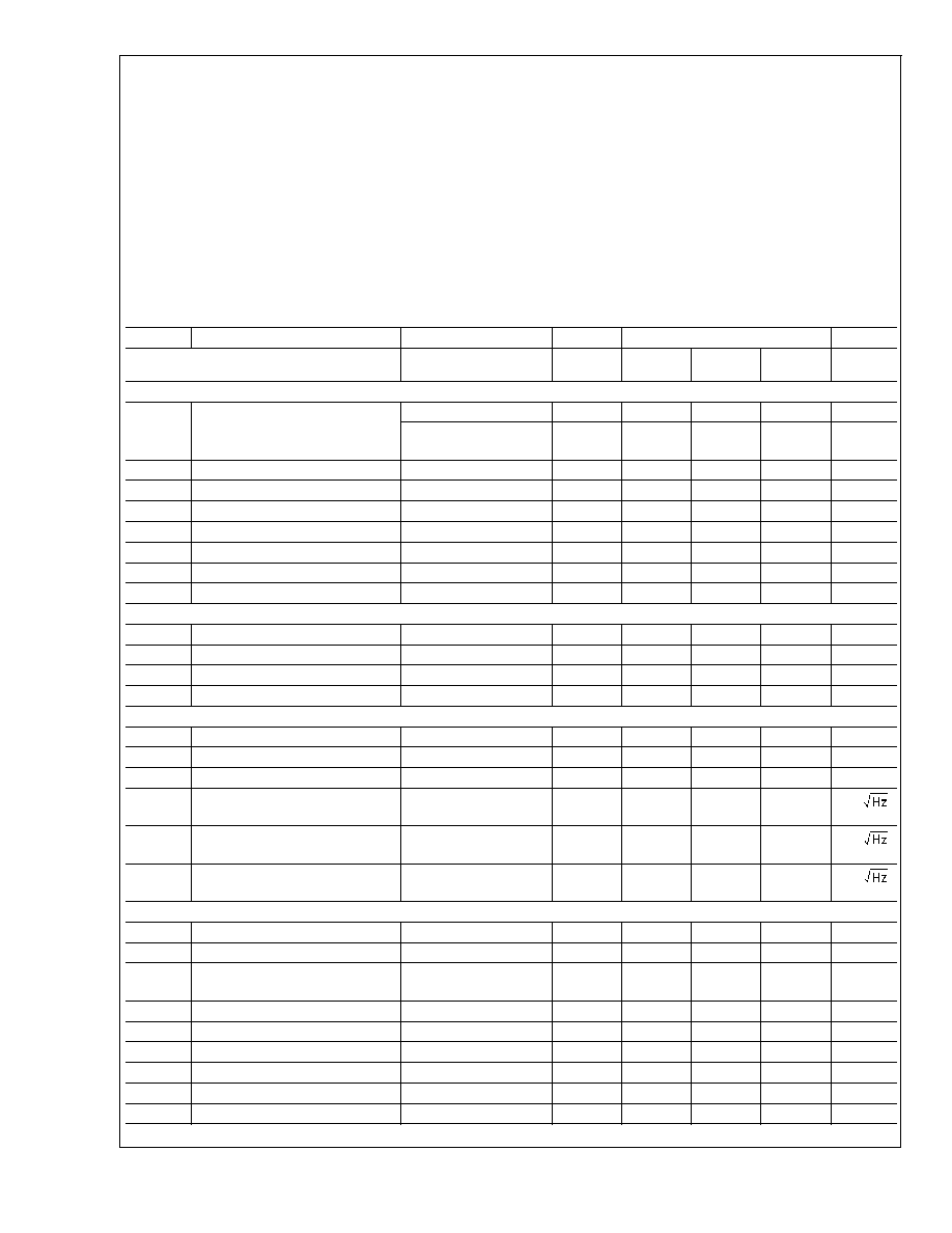
Electrical Characteristics
V
CC
=
±
15V; A
V
= +2; R
f
= R
g
= 750
; R
L
= 100
; unless noted
(Note 3)
Parameters
Conditions
Typ
Max/Min Ratings (Note 2)
Units
Ambient Temperature
CLC431 & CLC432
+25
+25
0 to +70
-40 to
+85
∞C
Frequency Domain Response
-3dB Bandwidth
V
OUT
<
4.0V
PP
62
42
37
36
MHz
V
OUT
<
4.0V
PP
, V
CC
=
±
5V
62
MHz
(Note 4)
V
OUT
<
10V
PP
28
21
20
20
MHz
Gain Flatness
V
OUT
<
4.0V
PP
Peaking
DC to 100MHz
0.05
0.5
0.7
0.7
dB
Rolloff
DC to 20MHz
0.0
0.8
0.8
0.8
dB
Linear Phase Deviation
DC to 30MHz
0.3
1.8
2.0
2.1
deg
Differential Gain
R
L
= 150
,4.43MHz
0.12
0.18
0.2
0.2
%
Differential Phase
R
L
= 150
, 4.43MHz
0.12
0.18
0.23
0.25
deg
Time Domain Response
(Note 4)
Rise and Fall Time
10V Step
8
12
13
13
ns
Overshoot
2V Step
5
10
12
12
%
Settling Time
2V Step to 0.05%
70
100
110
110
ns
(Note 4)
Slew Rate
V
OUT
=
±
10V
2000
1500
1450
1400
V/ms
Distortion And Noise Response
(Note 8)
2nd Harmonic Distortion
2V
PP
, 1MHz
-65
dBc
(Note 8)
3rd Harmonic Distortion
2V
PP
, 1MHz
-75
dBc
Equivalent Input Noise
Voltage
>
1MHz
3.3
4.2
4.4
4.5
nV/
Current, Inverting
>
1MHz
13
16
17
18
pA/
Current, Non-Inverting
>
1MHz
2.0
2.5
2.6
2.8
pA/
Static, DC Performance
(Note 9)
Input Offset Voltage
3
6
7
7
mV
Average Drift
20
-
50
50
µV/∞C
(Note 9)
Input Bias Current,
Non-Inverting
2
8
10
16
µA
Average Drift
25
-
100
150
nA/∞C
(Note 9)
Input Bias Current, Inverting
2
6
6
8
µA
Average Drift
8
-
25
40
nA/∞C
Power Supply Rejection Ratio
DC
64
59
59
59
dB
Common-Mode Rejection Ratio
DC
63
58
57
56
dB
(Note 9)
Supply Current
R
L
=
, Per Channel
7.1
7.9
8.5
9.6
mA
CLC431/432
www.national.com
4
Electrical Characteristics
(Continued)
V
CC
=
±
15V; A
V
= +2; R
f
= R
g
= 750
; R
L
= 100
; unless noted
(Note 3)
Parameters
Conditions
Typ
Max/Min Ratings (Note 2)
Units
Ambient Temperature
CLC431 & CLC432
+25
+25
0 to +70
-40 to
+85
∞C
Static, DC Performance
(Note 9)
CLC431
Disabled
R
L
=
, Per Channel
0.8
1.2
1.3
1.45
mA
Miscellaneous Performance
Input Voltage Range
Common Mode
±
12.2
±
12.0
±
11.8
±
11.6
V
Input Resistance
Non-Inverting
24
16
10
6
M
Input Capacitance
Non-Inverting
0.5
1
1
1
pF
Output Current
±
60
±
38
±
35
±
30
mA
Output Voltage Range
R
L
5k
±
14.0
±
13.6
±
13.4
±
13.2
V
R
L
= 100
±
6.0
±
3.7
±
3.7
±
2.9
V
Switching Performance (CLC431)
Switching Time
Turn On
0.1
0.15
0.155
0.165
µs
Turn Off
0.7
1.0
1.2
1.2
µs
(Note 5)
DIS Logic Levels
Single-Ended Mode
High Input Voltage (V
IH
)
>
2.0
>
2.0
>
2.0
>
2.0
V
Low Input Voltage (V
IL
)
<
0.8
<
0.8
<
0.8
<
0.8
V
Maximum Current Input
V
IH
>
DIS
>
V
IL
150
180
190
205
µA
(Note 6)
DIS-DIS
Differential Mode
Minimum Differential Voltage
0.3
0.4
0.4
0.4
V
Isolation
Crosstalk, Input Referred
10MHz
70
64
64
64
dB
(Note 7)
Off Isolation
10MHz
64
60
60
60
dB
Note 1: "Absolute Maximum Ratings" are those values beyond which the safety of the device cannot be guaranteed. They are not meant to imply that the devices
should be operated at these limits. The table of "Electrical Characteristics" specifies conditions of device operation.
Note 2: Min/max ratings are based on product characterization and simulation. Individual parameters are tested as noted. Outgoing quality levels are determined
from tested parameters.
Note 3: Tested and guaranteed with R
f
= 866
. CLC432 tested and guaranteed with R
f
= 750
Note 4: Spec is guaranteed for R
L
500
Note 5: V
RTTL
= 0, See text for single-ended mode of operation.
Note 6: V
RTTL
= NC, See text for differential mode operation.
Note 7: Spec is guaranteed for AJE & AJP yield 7dB lower
Note 8: Spec is tested with 2V
PP
, 10MHz and R
L
= 100
Note 9: J-level: spec is 100% tested at +25∞C
Typical Performance Characteristics
(T
A
= +25∞C, A
V
= +2, V
CC
=
±
15V, unless specified)
Non-Inverting Frequency Response
DS012712-6
Inverting Frequency Response
DS012712-7
CLC431/432
www.national.com
5