 | –≠–ª–µ–∫—Ç—Ä–æ–Ω–Ω—ã–π –∫–æ–º–ø–æ–Ω–µ–Ω—Ç: CLC440 | –°–∫–∞—á–∞—Ç—å:  PDF PDF  ZIP ZIP |
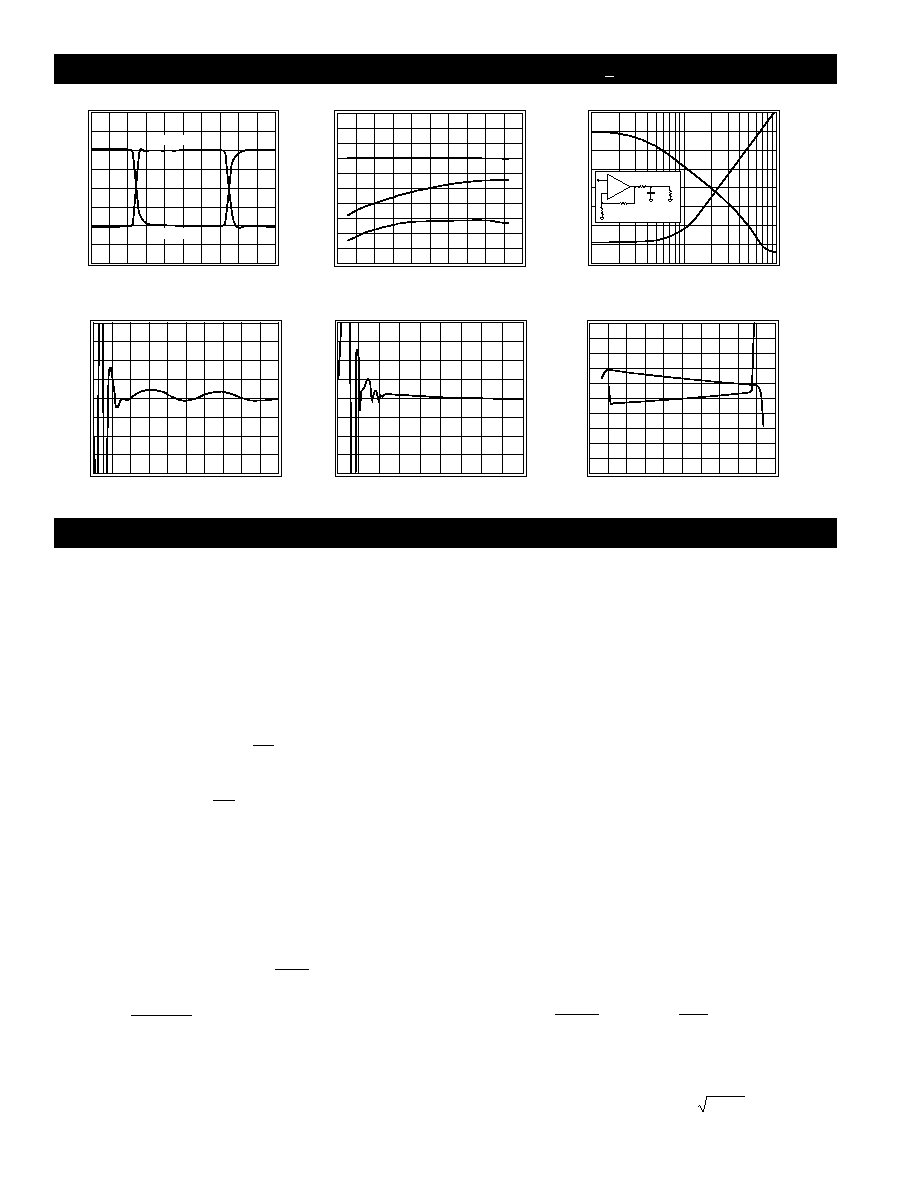
Frequency Response (A
V
= +2V/V)
Features
s
Unity-gain stable
s
High unity-gain bandwidth: 750MHz
s
Ultra-low differential gain: 0.015%
s
Very low differential phase: 0.025∞
s
Low power: 70mW
s
Extremely fast slew rate: 1500V/
µ
s
s
High output current: 90mA
s
Low noise: 3.5nV/
Hz
s
Dual ±2.5V to ±6V or single 5V to 12V supplies
Applications
s
Professional video
s
Graphics workstations
s
Test equipment
s
Video switching & routing
s
Communications
s
Medical imaging
s
A/D drivers
s
Photo diode transimpedance amplifiers
s
Improved replacement for CLC420 or OPA620
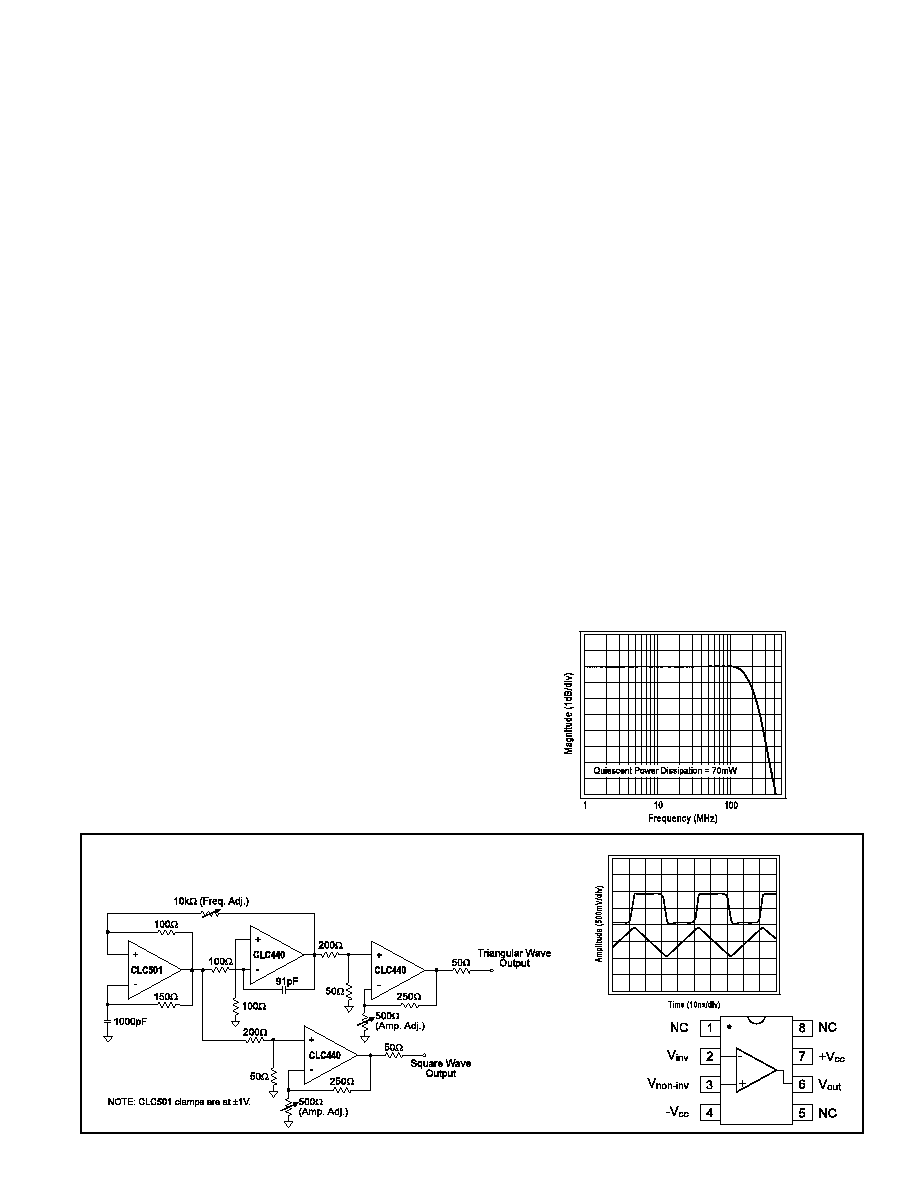
Typical Application
10MHz to 40MHz Square and Triangular Wave Generator
Pinout
DIP & SOIC
General Description
The CLC440 is a wideband, low-power, voltage feedback op amp
that offers 750MHz unity-gain bandwidth, 1500V/
µ
s slew rate, and
90mA output current. For video applications, the CLC440 sets new
standards for voltage feedback monolithics by offering the impres-
sive combination of 0.015% differential gain and 0.025∞ differen-
tial phase errors while dissipating a mere 70mW.
The CLC440 incorporates the proven properties of Comlinear's
current feedback amplifiers (high bandwidth, fast slewing, etc.) into a
"classical" voltage feedback architecture. This amplifier possesses
truly differential and fully symmetrical inputs both having a high
900k
impedance with matched low input bias currents.
Furthermore, since the CLC440 incorporates voltage feedback, a
specific R
f
is not required for stability. This flexibility in choosing R
f
allows for numerous applications in wideband filtering and integration.
Unlike several other high-speed voltage feedback op amps, the
CLC440 operates with a wide range of dual or single supplies
allowing for use in a multitude of applications with limited supply
availability. The CLC440's low 3.5nV/
Hz(e
n
) and 2.5pA/
Hz(i
n
)
noise sets a very low noise floor.
CLC440
High-Speed, Low-Power, Voltage Feedback Op Amp
N
June 1999
CLC440
High-Speed,
Lo
w-P
o
wer
,
V
olta
g
e
Feedbac
k Op Amp
Generator Waveforms
© 1999 National Semiconductor Corporation
http://www.national.com
Printed in the U.S.A.

PARAMETERS
CONDITIONS
TYP
MIN/MAX RATINGS
UNITS
NOTES
Ambient Temperature
CLC440
+25∞C
+25∞C
0 to 70∞C
-40 to 85∞C
FREQUENCY DOMAIN RESPONSE
-3dB bandwidth A
V
=+2
V
out
< 0.2V
pp
260
165
165
135
MHz
V
out
< 4.0V
pp
190
150
135
130
MHz
-3dB bandwidth A
V
=+1
V
out
< 0.2V
pp
750
MHz
gain bandwidth product
V
out
< 0.2V
pp
230
MHz
gain flatness
V
out
< 2.0V
pp
DC to 75MHz
0.05
0.15
0.20
0.20
dB
linear phase deviation
V
out
< 2.0V
pp
DC to 75MHz
0.8
1.2
1.5
1.5
deg
differential gain
4.43MHz, R
L
=150
0.015
0.03
0.04
0.04
%
differential phase
4.43MHz, R
L
=150
0.025
0.05
0.06
0.06
deg
TIME DOMAIN RESPONSE
rise and fall time
2V step
1.5
2.0
2.2
2.5
ns
4V step
3.2
4.2
4.5
5.0
ns
settling time to 0.05%
2V step
10
14
16
16
ns
overshoot
4V step
7
13
13
13
%
slew rate
4V step, ±0.5V crossing
1500
900
750
600
V/
µ
s
DISTORTION AND NOISE RESPONSE
2nd harmonic distortion
2V
pp
, 5MHz
-64
-59
-59
-59
dBc
2V
pp
, 20MHz
-52
-46
-46
-46
dBc
3rd harmonic distortion
2V
pp
, 5MHz
-70
-65
-64
-64
dBc
2V
pp
, 20MHz
-51
-45
-43
-43
dBc
equivalent input noise
voltage
>1MHz
3.5
4.5
5.0
5.0
nV/
Hz
current
>1MHz
2.5
3.5
4.0
4.0
pA/
Hz
STATIC DC PERFORMANCE
input offset voltage
1.0
3.0
3.5
4.0
mV
A
average drift
5.0
10
10
µ
V/∞C
input bias current
10
30
35
40
µ
A
A
average drift
30
50
60
nA/∞C
input offset current
0.5
2.0
2.0
3.0
µ
A
A
average drift
3.0
10
10
nA/∞C
power supply rejection ratio
DC
65
58
58
58
dB
common-mode rejection ratio
DC
80
65
60
60
dB
supply current
R
L
=
7.0
7.5
8.0
8.0
mA
A
MISCELLANEOUS PERFORMANCE
input resistance
common-mode
900
500
400
300
k
input capacitance
common-mode
1.2
2.0
2.0
2.0
pF
differential-mode
0.5
1.0
1.0
1.0
pF
input voltage range
common-mode
±3.0
±2.8
±2.7
±2.7
V
output voltage range
R
L
= 100
±2.5
±2.3
±2.2
±2.2
V
output voltage range
R
L
=
±3.0
±2.8
±2.7
±2.7
V
output current
±80
±72
±65
±45
mA
Min/max ratings are based on product characterization and simulation. Individual parameters are tested as noted. Outgoing quality levels are
determined from tested parameters.
CLC440 Electrical Characteristics
(A
V
= +2, R
f
= R
g
= 250
: V
cc
= + 5V, R
L
= 100
unless specified)
Absolute Maximum Ratings
voltage supply
±6V
I
out
is short circuit protected to ground
common-mode input voltage
±Vcc
maximum junction temperature
+150∞C
storage temperature range
-65∞C to +150∞C
lead temperature (soldering 10 sec)
+300∞C
ESD rating (human bodey model)
<1000V
Notes
A) J-level: spec is 100% tested at +25∞C.
Transitor Count
46
Ordering Information
Model
Temperature Range
Description
CLC440AJP
-40
∞
C to +85
∞
C
8-pin PDIP
CLC440AJE
-40
∞
C to +85
∞
C
8-pin SOIC
CLC440A8B
-55
∞
C to +125
∞
C
8-pin hermetic CerDIP,
MIL-STD-883
Contact factory for SMD number.
Package Thermal Resistance
Package
jc
ja
Plastic (AJP)
70
∞
/W
125
∞
/W
Surface Mount (AJE)
60
∞
/W
140
∞
/W
CerDip
40
∞
/W
130
∞
/W
http://www.national.com
2

CLC440 Typical Performance Characteristics
(A
V
= +2, R
f
= 250
: V
cc
= + 5V, R
L
= 100
unless specified)
Non-Inverting Frequency Response
Magnitude (1dB/div)
Phase (deg)
-180
-90
-135
-45
0
1
10
100
Frequency (MHz)
A
V
= 10
A
V
= 2
A
V
= 1
A
V
= 1(R
f
= 0)
A
V
= 2
A
V
= 10
A
V
= 5
A
V
= 5
1000
Gain
Phase
Inverting Frequency Response
Magnitude (1dB/div)
Phase (deg)
-360
-270
-315
-225
-180
1
10
100
Frequency (MHz)
A
V
-10
A
V
-1
A
V
-2
A
V
= -1
A
V
= -2
A
V
= -10
(Rf = 500
)
A
V
= -5
A
V
-5
1000
Gain
Phase
Frequency Response vs. Load
Magnitude (1dB/div)
Phase (deg)
-180
-90
-135
-45
0
1
10
100
Frequency (MHz)
R
L
=1K
R
L
=100
R
L
=1K
R
L
=100
R
L
=50
R
L
=50
1000
Gain
Phase
Frequency Response vs. V
out
Magnitude (1dB/div)
Phase (deg)
-180
-90
-135
-45
0
1
10
100
Frequency (MHz)
V
out
= 200mV
pp
1000
Gain
Phase
V
out
= 2V
pp
V
out
= 5V
pp
V
out
= 5V
pp
V
out
= 200mV
pp
V
out
= 2V
pp
Frequency Response vs. Capacitive Load
Magnitude (1dB/div)
Phase (deg)
-180
-90
-135
-45
0
1
10
100
Frequency (MHz)
C
L
= 10pF
R
s
= 50
1000
Gain
Phase
C
L
= 100pF
R
s
= 30
C
L
= 1000pF
R
s
= 5
C
L
= 1000pF
C
L
= 100pF
C
L
= 10pF
+
-
R
s
1k
C
L
Gain Flatness and Linear Phase
Magnitude (0.05dB/div)
Phase (1.0deg/div)
0
Frequency (7.5MHz/div)
75
Gain
Phase
Open Loop Gain and Phase
Open Loop Gain (dB)
Phase (deg)
1k
Frequency (Hz)
100M
Gain
Phase
10k
100k
1M
10M
80
60
40
20
0
-20
0
-90
-180
-270
BW vs. Gain for Transimpedance Configuration
C
f
(pF)
100
1000
10000
R
f
0
4
8
16
20
Bandwidth (MHz)
400
320
240
80
0
12
160
Cd = 1pF
Cd = 5pF
Cd = 20pF
BW
C
f
R
f
1000
C
f
1.6
BW
123
See dashed lines
Example
Equivalent Input Noise
Noise Voltage (nV/
Hz)
Frequency (Hz)
10
1
1k
100
10k
100k
1M
10M
Noise Current (pA/
Hz)
10
1
Voltage = 3.5nV/
Hz
Current = 2.5pA/
Hz
100M
Harmonic Distortion vs. Frequency
Distortion (dBc)
Frequency (MHz)
-45
-55
-95
0.1
1
10
-75
-85
-65
3rd R
L
= 100
2nd R
L
= 1k
3rd R
L
= 1k
2nd R
L
= 100
50
V
o
= 2V
pp
1dB Compression
Gain (1dB/div)
Output Power (P
out
)
-4
0
16
50MHz
100MHz
5MHz
20MHz
4
8
12
+
-
50
50
P
out
250
250
Input and Output VSWR
VSWR
Frequency (20MHz/div)
0
200
Input
Output
1.0
1.4
1.8
2.2
40
80
120
160
+
-
50
Output
50
250
50
Input
PSRR, CMRR, and Closed Loop R
out
PSRR/CMRR (dB)
Frequency (Hz)
45
35
10k
100k
100M
15
25
100
80
40
0
60
5
1M
10M
20
CMRR
R
out
PSRR
R
out
(
)
Differential Gain and Phase
Differential Gain (%), Phase (deg)
Number of 150
Loads
0.12
1
2
3
0.04
0
0.08
Gain
Positive Sync
Phase
Negative Sync
4
Gain
Negative Sync
Phase
Positive Sync
2-Tone, 3rd Order Intermodulation Intercept
Intercept Point (+dBm)
1
10
100
Frequency (MHz)
50
40
30
20
10
0
+
-
50
P
out
250
250
50
3
http://www.national.com
General Design Equations
The CLC440 is a unity gain stable voltage feedback
amplifier. The matched input bias currents track well over
temperature. This allows the DC offset to be minimized
by matching the impedance seen by both inputs.
Gain
The non-inverting and inverting gain equations for the
CLC440 are as follows:
Non-inverting Gain:
Inverting Gain:
Gain Bandwidth Product
The CLC440 is a voltage feedback amplifier, whose
closed-loop bandwidth is approximately equal to the
gain-bandwidth product (GBP) divided by the gain (Av).
For gains greater than 5, Av sets the closed-loop band-
width of the CLC440.
Closed Loop Bandwidth =
GBP = 230MHz
For gains less than 5, refer to the frequency response
plots to determine maximum bandwidth.
Output Drive and Settling Time Performance
The CLC440 has large output current capability. The
90mA of output current makes the CLC440 an excellent
choice for applications such as:
∑
Video Line Drivers
∑
Distribution Amplifiers
When driving a capacitive load or coaxial cable, include a
series resistance Rs to back match or improve settling
time. Refer to the "Settling Time vs. Capacitive Load" plot
in the typical performance section to determine the
recommended resistance for various capacitive loads.
When driving resistive loads of under 500
, settling time
performance diminishes. This degradation occurs
because a small change in voltage on the output causes
a large change of current in the power supplies. This
current creates ringing on the power supplies. A small
resistor will dampen this effect if placed in series with the
6.8
µ
F bypass capacitor.
Noise Figure
Noise Figure (NF) is a measure of noise degradation
caused by an amplifier.
where,
e
ni
= Total Equivalent Input Noise Density
Due to the Amplifier
e
t
= Thermal Voltage Noise (
seq
)
CLC440 Typical Performance Characteristics
(A
V
= +2, R
f
= 250
: V
cc
= + 5V, R
L
= 100
unless specified)
I
b
and I
os
vs. Common-Mode Voltage
Offset Current, I
os
(5nA/div
)
Bias Current, I
b
(0.5
µ
A/div)
Common-Mode Input Voltage (V)
-4.0
-2.4
2.4
0
4.0
0
-0.8
0.8
I
b
l
os
-10
-20
10
20
2.0
1.0
-1.0
-2.0
APPLICATION INFORMATION
Pulse Response
Output Voltage (0.5V/div)
Time (5ns/div)
2.0
1.0
-1.0
-2.0
0
A
V
= +2
A
V
= -2
0.05% Settling Time vs. Capacitive Load
Settling Time, T
s
(ns) to 0.05%
10
100
1000
Load Capacitance C
L
(pF)
80
60
40
20
0
Recommended R
s
(
)
55
45
35
25
15
+
-
R
s
1k
C
L
R
s
T
s
Short Term Settling Time
Settling Error % of Output Step
Time (ns)
0
20
80
0.1
100
40
60
0.2
0
-0.1
-0.2
Long Term Settling Time
Settling Error % of Output Step
Time (s)
10
-9
10
-7
10
-1
0.1
10
0
10
-5
10
-3
0.2
0
-0.1
-0.2
10
-2
10
-4
10
-6
10
-8
1
R
R
f
g
+
-
R
R
f
g
GBP
A
v
A
R
R
R
v
f
g
g
=
+
(
)
NF
10LOG
S /N
S /N
10LOG
e
e
i
i
o
o
ni
2
t
2
=
=
4kTR
Typical DC Errors vs. Temperature
Input Offset Voltage, V
io
(mV)
Input Bias, Offset Current, l
b
l
os
(
µ
A)
Temperature (C
∞
)
0.4
0
-60
-20
100
-0.8
-1.6
-0.4
140
6
2
-6
-14
-2
-1.2
20
60
-10
l
os
l
b
V
io
http://www.national.com
4
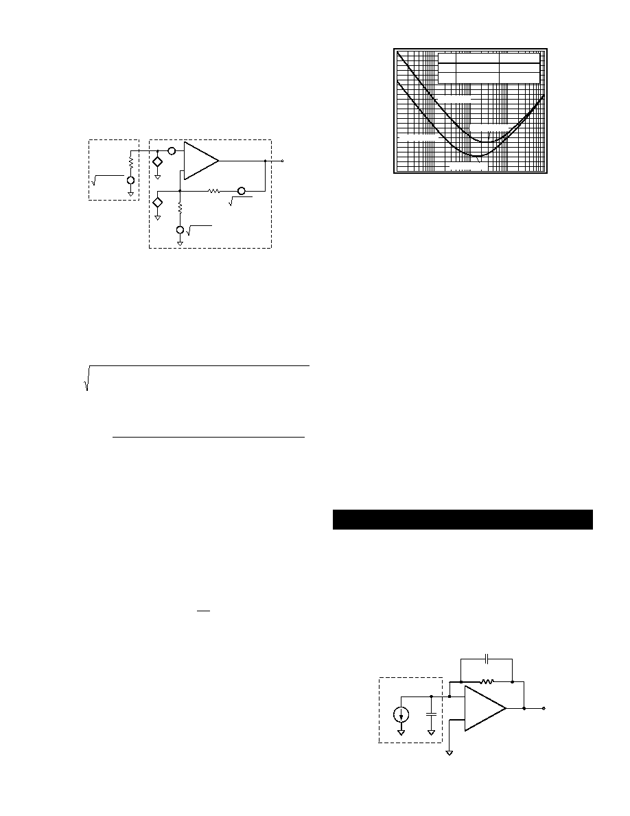
Figure 1 shows the noise model for the non-inverting
amplifier configuration. The model includes all of the
following noise sources:
∑
Input voltage noise (e
n
)
∑
Input current noise (i
n
= i
n+
= i
n-
)
∑
Thermal Voltage Noise (e
t
) associated with each
external resistor
Figure 1: Non-inverting Amplifier Noise Model
The total equivalent input noise density is calculated
by using the noise model shown. Equations 1 and 2
represent the noise equation and the resulting equation
for noise figure.
Equation 1: Noise Equation
Equation 2: Noise Figure Equation
The noise figure is related to the equivalent source
resistance (R
seq
) and the parallel combination of R
f
and
R
g.
To minimize noise figure, the following steps are
recommended:
∑
Minimize R
f
IIR
g
∑
Choose the optimum R
s
(R
OPT
)
R
OPT
is the point at which the NF curve reaches a
minimum and is approximated by:
Figure 2 is a plot of NF vs R
s
with R
f
= 0, R
g
=
(A
v
= +1).
The NF curves for both Unterminated and Terminated
systems are shown. The Terminated curve assumes R
s
= R
T
. The table indicates the NF for various source resis-
tances including R
s
= R
OPT
.
Layout Considerations
A proper printed circuit layout is essential for achieving
high frequency performance.
National provides
evaluation boards for the CLC440 (CLC730055-DIP,
CLC730060-SOIC) and suggests their use as a guide for
high frequency layout and as an aid in device testing and
characterization.
Figure 2: Noise Figure vs. Source Resistance
These boards were laid out for optimum, high-speed
performance. The ground plane was removed near the
input and output pins to reduce parasitic capacitance.
And all trace lengths were minimized to reduce series
inductances.
Supply bypassing is required for the amplifiers
performance.
The bypass capacitors provide a low
impedance return current path at the supply pins. They
also provide high frequency filtering on the power supply
traces. 6.8
µ
F tantalum, 0.01
µ
F ceramic, and 500pF
ceramic capacitors are recommended on both supplies.
Place the 6.8
µ
F capacitors within 0.75 inches of the
power pins, and the 0.01
µ
F and 500pF capacitors less
than 0.1 inches from the power pins.
Dip sockets add parasitic capacitance and inductance
which can cause peaking in the frequency response and
overshoot in the time domain response. If sockets are
necessary, flush-mount socket pins are recommended.
The device holes in the 730055 evaluation board are
sized for Cambion P/N 450-2598 socket pins, or their
functional equivalent.
Transimpedance Amplifier
The low 2.5pA/
Hz input current noise and unity gain
stability make the CLC440 an excellent choice for
transimpedance applications.
Figure 3 illustrates a
low noise transimpedance amplifier that is commonly
implemented with photo diodes. R
f
sets the transimped-
ance gain. The photo diode current multiplied by R
f
determines the output voltage.
Figure 3: Transimpedance Amplifier Configuration
R
seq
R
f
+
-
R
g
CLC440
*
i
n+
*
*
e
n
i
n-
*
*
*
4kTRseq
4kTR
f
4kTRg
R
seq
= R
s
for Unterminated Systems
R
seq
= R
s
II R
T
for Terminated Systems
Noise Figure vs. Source Resistance
Noise Figure (dB)
Source Resistance (
)
10
100k
Unterminated
Terminated
10
15
20
25
100
1k
10k
5
0
R
opt
= 2800
R
opt
= 1400
R
s
(
)
50
R
OPT
NF Unterminated
12.03dB
3.13dB
NF Terminated
17.90dB
6.15dB
Applications Circuits
I
in
-
+
CLC440
C
d
R
f
C
f
Photo Diode
Representation
V
out
= -I
in
*R
f
V
out
e
e
i
R
R IIR
4kTR
4kT R IIR
ni
n
2
n
2
seq
2
f
g
2
seq
f
g
=
+
+
(
)
+
+
(
)
NF
10LOG
e
i
R
R IIR
4kTR
4kT R IIR
4kTR
n
2
n
2
seq
2
f
g
2
seq
f
g
seq
=
+
+
(
)
+
+
(
)
R
e
i
OPT
n
n
5
http://www.national.com