 | –≠–ª–µ–∫—Ç—Ä–æ–Ω–Ω—ã–π –∫–æ–º–ø–æ–Ω–µ–Ω—Ç: CLC440AM | –°–∫–∞—á–∞—Ç—å:  PDF PDF  ZIP ZIP |

CLC440
High Speed, Low Power, Voltage Feedback Op Amp
General Description
The CLC440 is a wideband, low power, voltage feedback op
amp that offers 750MHz unity-gain bandwidth, 1500V/µs
slew rate, and 90mA output current. For video applications,
the CLC440 sets new standards for voltage feedback
monolithics by offering the impressive combination of
0.015% differential gain and 0.025∞ differential phase errors
while dissipating a mere 70mW.
The
CLC440
incorporates
the
proven
properties
of
Comlinear's current feedback amplifiers (high bandwidth,
fast slewing, etc.) into a "classical" voltage feedback
architecture. This amplifier possesses truly differential and
fully
symmetrical
inputs
both
having
a
high
900k
impedance
with
matched
low
input
bias
currents.
Furthermore,
since
the
CLC440
incorporates
voltage
feedback, a specific R
f
is not required for stability. This
flexibility in choosing R
f
allows for numerous applications in
wideband filtering and integration.
Unlike several other high speed voltage feedback op amps,
the CLC440 operates with a wide range of dual or single
supplies allowing for use in a multitude of applications with
limited supply availability. The CLC440's low 3.5nV/
(e
n
)
and 2.5pA/
(i
n
) noise sets a very low noise floor.
Features
n
Unity-gain stable
n
High unity-gain bandwidth: 750MHz
n
Ultra low differential gain: 0.015%
n
Very low differential phase: 0.025∞
n
Low power: 70mW
n
Extremely fast slew rate: 1500V/µs
n
High output current: 90mA
n
Low noise: 3.5nV/
n
Dual
±
2.5V to
±
6V or single 5V to 12V supplies
Applications
n
Professional video
n
Graphics workstations
n
Test equipment
n
Video switching & routing
n
Communications
n
Medical imaging
n
A/D drivers
n
Photo diode transimpedance amplifiers
n
Improved replacement for CLC420 or OPA620
Connection Diagram
Frequency Response (A
V
= +2V/V)
DS012714-1
Generator Waveforms
DS012714-25
DS012714-26
Pinout
DIP & SOIC
February 2001
CLC440
High
Speed,
Low
Power
,
V
oltage
Feedback
Op
Amp
© 2001 National Semiconductor Corporation
DS012714
www.national.com

Typical Application
Ordering Information
Package
Temperature Range
Industrial
Part Number
Package Marking
NSC Drawing
8-pin plastic DIP
-40∞C to +85∞C
CLC440AJP
CLC440AJP
N08E
8-pin plastic SOIC
-40∞C to +85∞C
CLC440AJE
CLC440AJE
M08A
DS012714-2
CLC440
www.national.com
2

Absolute Maximum Ratings
(Note 1)
If Military/Aerospace specified devices are required,
please contact the National Semiconductor Sales
Office/Distributors for availability and specifications.
Supply Voltage (V
CC
)
±
6V
I
OUT
is short circuit protected to
ground
Common Mode Input Voltage
±
V
CC
Maximum Junction Temperature
+150∞C
Storage Temperature Range
-65∞C to +150∞C
Lead Temperature (soldering, 10 sec)
+300∞C
ESD rating (human body model)
<
1000V
Operating Ratings
Thermal Resistance
Package
(
JC
)
(
JA
)
MDIP
70∞C/W
125∞C/W
SOIC
60∞C/W
140∞C/W
Electrical Characteristics
A
V
= +2, R
f
= R
g
= 250
; V
CC
=
±
5V, R
L
= 100
unless specified.
Symbol
Parameter
Conditions
Typ
Min/Max (Note 2)
Units
Ambient Temperature
CLC440IN
+25∞C
+25∞C
0 to
70∞C
-40 to
85∞C
Frequency Domain Response
-3dB Bandwidth A
V
= +2
V
OUT
<
0.2V
PP
260
165
165
135
MHz
V
OUT
<
4.0V
PP
190
150
135
130
MHz
-3dB Bandwidth A
V
= +1
V
OUT
<
0.2V
PP
750
MHz
Gain Bandwidth Product
V
OUT
<
0.2V
PP
230
MHz
Gain Flatness
V
OUT
<
2.0V
PP
, DC to 75MHz
0.05
0.15
0.20
0.20
dB
Linear Phase Deviation
V
OUT
<
2.0V
PP
, DC to 75MHz
0.8
1.2
1.5
1.5
deg
Differential Gain
R
L
=150
, 4.43MHz
0.015
0.03
0.04
0.04
%
Differential Phase
R
L
=150
, 4.43MHz
0.025
0.05
0.06
0.06
deg
Time Domain Response
Rise and Fall Time
2V step
1.5
2.0
2.2
2.5
ns
4V step
3.2
4.2
4.5
5.0
ns
Settling Time to
±
0.05%
2V step
10
14
16
16
ns
Overshoot
4V step
7
13
13
13
%
Slew Rate
4V step,
±
0.5V crossing
1500
900
750
600
V/µs
Distortion And Noise Response
2nd Harmonic Distortion
2V
PP
, 5MHz
-64
-59
-59
-59
dBc
2V
PP
, 20MHz
-52
-46
-46
-46
dBc
3rd Harmonic Distortion
2V
PP
, 5MHz
-70
-65
-64
-64
dBc
2V
PP
, 20MHz
-51
-45
-43
-43
dBc
Equivalent Input Noise
Voltage
>
1MHz
3.5
4.5
5.0
5.0
nV/
Current
>
1MHz
2.5
3.5
4.0
4.0
pA/
Static DC Performance
Input Offset Voltage (Note 3)
1.0
3.0
3.5
4.0
mV
Average Drift
5.0
-
10
10
µV/∞C
Input Bias Current (Note 3)
10
30
35
40
µA
Average Drift
30
-
50
60
nA/∞C
Input Offset Current (Note 3)
0.5
2.0
2.0
3.0
µA
Average Drift
3.0
-
10
10
nA/∞C
Power Supply Rejection Ratio
DC
65
58
58
58
dB
Common Mode Rejection Ratio
DC
80
65
60
60
dB
Supply Current (Note 3)
R
L
=
7.0
7.5
8.0
8.0
mA
Miscellaneous Performance
Input Resistance
Common-Mode
900
500
400
300
k
CLC440
www.national.com
3
Electrical Characteristics
(Continued)
A
V
= +2, R
f
= R
g
= 250
; V
CC
=
±
5V, R
L
= 100
unless specified.
Symbol
Parameter
Conditions
Typ
Min/Max (Note 2)
Units
Miscellaneous Performance
Input Capacitance
Common-Mode
1.2
2.0
2.0
2.0
pF
Differential-Mode
0.5
1.0
1.0
1.0
pF
Input Voltage Range
Common-Mode
±
3.0
±
2.8
±
2.7
±
2.7
V
Output Voltage Range
R
L
= 100
±
2.5
±
2.3
±
2.2
±
2.2
V
Output Voltage Range
R
L
=
±
3.0
±
2.8
±
2.7
±
2.7
V
Output Current
±
80
±
72
±
65
±
45
mA
Note 1: "Absolute Maximum Ratings" are those values beyond which the safety of the device cannot be guaranteed. They are not meant to imply that the devices
should be operated at these limits. The table of "Electrical Characteristics" specifies conditions of device operation.
Note 2: Min/max ratings are based on product characterization and simulation. Individual parameters are tested as noted. Outgoing quality levels are determined
from tested parameters.
Note 3: AJ-level: spec. is 100% tested at +25∞C.
Typical Performance Characteristics
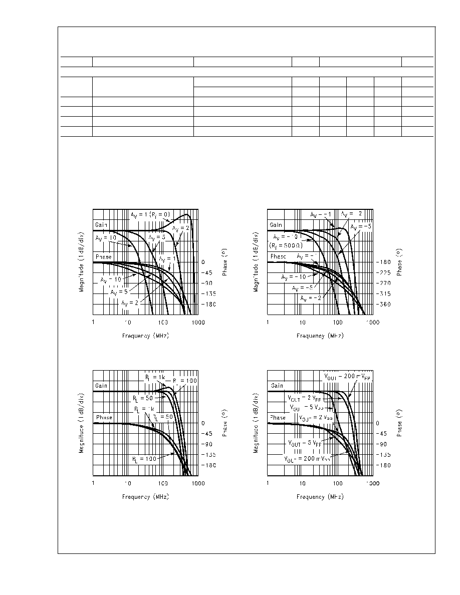
Non-Inverting Frequency Response
DS012714-3
Inverting Frequency Response
DS012714-4
Frequency Response vs. Load
DS012714-5
Frequency Response vs. V
OUT
DS012714-6
CLC440
www.national.com
4

Typical Performance Characteristics
(Continued)
Frequency Response vs. Capacitive Load
DS012714-7
Gain Flatness and Linear Phase
DS012714-41
Open Loop Gain and Phase
DS012714-8
BW vs. Gain for Transimpedance Configuration
DS012714-9
Equivalent Input Noise
DS012714-10
Harmonic Distortion vs. Frequency
DS012714-11
CLC440
www.national.com
5