 | –≠–ª–µ–∫—Ç—Ä–æ–Ω–Ω—ã–π –∫–æ–º–ø–æ–Ω–µ–Ω—Ç: CLC446 | –°–∫–∞—á–∞—Ç—å:  PDF PDF  ZIP ZIP |

Features
s
400MHz bandwidth (A
v
= +2)
s
5mA supply current
s
0.02%, 0.03∞ differential gain, phase
s
2000V/
µ
s slew rate
s
9ns settling to 0.1%
s
0.05dB gain flatness to 100MHz
s
-65/-78dBc HD2/HD3
Applications
s
High resolution video
s
A/D driver
s
Medical imaging
s
Video switchers & routers
s
RF/IF amplifier
s
Communications
s
Instrumentation
General Description
The National CLC446 is a very high-speed unity-gain-stable cur-
rent-feedback op amp that is designed to deliver the highest lev-
els of performance from a mere 50mW quiescent power. It pro-
vides a very wide 400MHz bandwidth, a 2000V/
µ
s slew rate and
900ps rise/fall times. The CLC446 achieves its superior speed-
vs-power using an advanced complementary bipolar IC process
and National's current-feedback architecture.
The CLC446 is designed to drive video loads with very low
differential gain and phase errors (0.02%, 0.03∞). Combined with
its very low power (50mW), the CLC446 makes an excellent
choice for NTSC/PAL video switchers and routers. With its very
quick edge rates (900ps) and high slew rate (2000V/
µ
s), the
CLC446 also makes an excellent choice for high-speed, high-
resolution component RGB video systems.
The CLC446 makes an excellent low-power high-resolution A/D
converter driver with its very fast 9ns settling time (to 0.1%) and
low harmonic distortion.
The combination of high performance and low power make
the CLC446 useful in many high-speed general purpose
applications. Its current-feedback architecture maintains consistent
performance over a wide gain range and signal levels. DC gain
and bandwidth can be set independently. Also, either maximally
flat AC response or linear phase response can be emphasized.
V
in
R
4
R
f
+
-
R
g
C
2
CLC446
C
5
V
o
R
5
R
1
R
2
C
3
C
4
R
3
C
1
Typical Application
Elliptic-Function Low Pass Filter
CLC446
400MHz, 50mW Current-Feedback Op Amp
Non-Inverting
Frequency Response (A
v
= +2)
Gain (dB)
Frequency (Hz)
8
6
1M
1G
2
-2
4
0
10M
100M
V
o
= 0.5V
pp
V
EE
V
CC
Pinout
DIP & SOIC
November 1998
CLC446
400MHz, 50mW Current-Feedback Op
Amp
N
© 1998 National Semiconductor Corporation
http://www.national.com
Printed in the U.S.A.
http://www.national.com
2
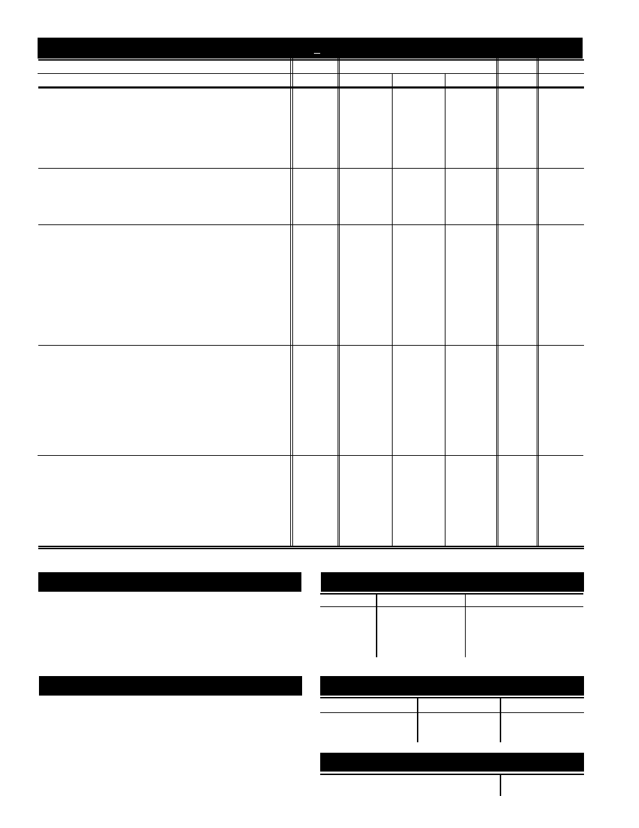
Electrical Characteristics
(A
V
= +2, R
f
= 249
: V
CC
= + 5V, R
L
= 100
;
unless specified)
PARAMETERS
CONDITIONS
TYP
MIN/MAX RATINGS
UNITS
NOTES
Ambient Temperature
CLC446AJ
+25∞C
+25∞C
0 to 70∞C
-40 to 85∞C
FREQUENCY DOMAIN RESPONSE
-3dB bandwidth
V
o
< 0.2V
pp
400
340
300
300
MHz
V
o
< 2.0V
pp
280
210
190
190
MHz
gain flatness
V
o
< 2.0V
pp
<100MHz
±0.05
±0.2
±0.2
±0.2
dB
linear phase dev. V
o
< 2.0V
pp
<100MHz
0.2
0.5
0.8
0.8
deg
differential gain
NTSC, R
L
=150
0.02
0.04
0.04
0.04
%
differential phase
NTSC, R
L
=150
0.03
0.05
0.05
0.05
deg
TIME DOMAIN RESPONSE
rise and fall time
2V step
0.9
1.4
1.5
1.6
ns
settling time to 0.1%
2V step
9
13
15
15
ns
overshoot
2V step
6
15
18
18
%
slew rate
2V step, ±0.5V crossing
2000
1400
1300
1200
V/
µ
s
DISTORTION AND NOISE RESPONSE
2
nd
harmonic distortion
2V
pp
, 5MHz
-65
-59
-58
-58
dBc
2V
pp
, 20MHz
-55
-48
-48
-48
dBc
2V
pp
, 50MHz
-54
-43
-42
-42
dBc
3
rd
harmonic distortion
2V
pp
, 5MHz
-78
-70
-68
-68
dBc
2V
pp
, 20MHz
-70
-62
-60
-60
dBc
2V
pp
, 50MHz
-50
-45
-42
-42
dBc
equivalent input noise
voltage (e
ni
)
>1MHz
3.8
4.8
5.0
5.1
nV/
Hz
non-inverting current (i
bn
)
>1MHz
2.0
2.6
2.8
3.3
pA/
Hz
inverting current (i
bi
)
>1MHz
16
19
20
21
pA/
Hz
STATIC DC PERFORMANCE
input offset voltage
2
7
10
11
mV
A
average drift
17
≠
25
35
µ
V/∞C
input bias current
non-inverting
3
12
25
25
µ
A
A
average drift
30
≠
90
130
nA/∞C
input bias current
inverting
10
22
30
35
µ
A
A
average drift
26
≠
75
85
nA/∞C
power supply rejection ratio
DC
52
45
43
43
dB
common-mode rejection ratio
DC
48
44
42
42
dB
supply current
R
L
=
4.8
5.8
6.2
6.2
mA
A
MISCELLANEOUS PERFORMANCE
input resistance
non-inverting
1.5
1.0
0.85
0.70
M
input capacitance
non-inverting
1
2
2
2
pF
input range
common-mode
±2.8
±2.6
±2.4
±2.3
V
output voltage range
R
L
= 100
±3.1
±2.8
±2.8
±2.6
V
R
L
=
±3.2
±3.0
±2.9
±2.8
V
output current
48
48
48
48
mA
output resistance, closed loop
DC
0.04
0.1
0.1
0.1
Min/max ratings are based on product characterization and simulation. Individual parameters are tested as noted. Outgoing quality levels are
determined from tested parameters.
Absolute Maximum Ratings
supply voltage
±6V
output current
±48mA
common-mode input voltage
±Vcc
maximum junction temperature
+175∞C
storage temperature range
-65∞C to +150∞C
lead temperature (soldering 10 sec)
+300∞C
ESD rating (human body model)
1000V
Notes
A) J-level: spec is 100% tested at +25∞C.
Ordering Information
Model
Temperature Range
Description
CLC446AJP
-40
∞
C to +85
∞
C
8-pin PDIP
CLC446AJE
-40
∞
C to +85
∞
C
8-pin SOIC
CLC446ALC
-40
∞
C to +85
∞
C
dice
CLC446A8B
-55
∞
C to +125
∞
C
8-pin CerDIP, MIL-STD-883
CLC446AMC
-55
∞
C to +125
∞
C
dice, MIL-STD-883
Contact the factory for other packages and DESC SMD number.
Package Thermal Resistance
Package
JC
JA
Plastic (AJP)
70∞C/W
125∞C/W
Surface Mount (AJE)
60∞C/W
140∞C/W
Ceramic (A8B)
40∞C/W
130∞C/W
Reliability Information
Transistor Count
36
MTBF (based on limited test data)
39Mhr

3
http://www.national.com
Typical Performance Characteristics
(V
CC
= ±5V, A
v
= +2, R
f
=249
,,
R
L
= 100
; unless specified)
Non-Inverting Frequency Response
Normalized Magnitude (1dB/div)
Frequency (Hz)
10M
100M
1G
V
o
= 0.5V
pp
Phase (deg)
0
-90
-360
-180
-270
-450
1M
A
v
= 1V/V
R
f
= 453
A
v
= 2V/V
R
f
= 249
A
v
= 5V/V
R
f
= 200
A
v
= 10V/V
R
f
= 200
Inverting Frequency Response
Normalized Magnitude (1dB/div)
Frequency (Hz)
1M
10M
1G
Phase (deg)
-180
-225
-360
-270
-315
100M
V
o
= 0.5V
pp
A
v
= -1V/V
R
f
= 249
A
v
= -2V/V
R
f
= 249
A
v
= -5V/V
R
f
= 200
A
v
= -10V/V
R
f
= 200
Frequency Response vs. R
L
Normalized Magnitude (1dB/div)
Frequency (Hz)
10M
100M
1G
Phase (deg)
0
-90
-360
-180
-270
-450
1M
R
L
= 1k
R
L
= 100
R
L
= 500
V
o
= 0.5V
pp
Frequency Response vs. V
o
Normalized Magnitude (1dB/div)
Frequency (Hz)
1M
10M
100M
1G
0.1V
pp
1V
pp
4V
pp
2V
pp
Frequency Response vs. C
L
Normalized Magnitude (1dB/div)
Frequency (Hz)
1M
10M
100M
1G
C
L
= 22pF
R
s
= 33.2
C
L
= 10pF
R
s
= 46.4
C
L
= 47pF
R
s
= 21
C
L
= 100pF
R
s
= 13.3
C
L
1k
R
s
+
-
249
249
Recommended R
s
vs. C
L
R
s
(
)
C
L
(pF)
40
30
0
10
20
100
20
10
30
40
50
60
70
80
90
50
Small Signal Pulse Response
Output Voltage (0.5V/div)
Time (2ns/div)
A
v
=
+
2V/V
A
v
=
-
2V/V
Large Signal Pulse Response
Output Voltage (1V/div)
Time (2ns/div)
A
v
=
-
2V/V
A
v
=
+
2V/V
Equivalent Input Noise
Voltage Noise (nV/
Hz)
Frequency (Hz)
100
1
1k
10k
100k
10
Current Noise (pA/
Hz)
100
1
10
1M
10M
i
bi
e
ni
i
bn
100M
2nd Harmonic Distortion
Distortion (dBc)
Frequency (Hz)
-50
-60
-90
1M
10M
-70
-80
V
o
= 2V
pp
-100
2nd R
L
= 100
2nd R
L
= 1k
3rd Harmonic Distortion
Distortion (dBc)
Frequency (Hz)
-60
-70
-100
1M
10M
-80
-90
V
o
= 2V
pp
-50
3rd R
L
= 100
3rd R
L
= 1k
Differential Gain and Phase (3.58MHz)
Differential Gain (%)
Number of 150
Loads
0.01
0
-0.03
1
2
3
-0.01
-0.02
Differential Phase (deg)
-0.04
-0.08
-0.2
-0.12
-0.16
-0.04
0
4
Phase Pos Sync
Phase Neg Sync
Gain Pos Sync
Gain Neg Sync
2nd Harmonic Distortion vs. P
out
Distortion (dBc)
Output Power (dBm)
-40
-50
-80
-4
-2
0
-60
-70
2
4
6
8
10
12
10MHz
5MHz
2MHz
1MHz
3rd Harmonic Distortion vs. P
out
Distortion (dBc)
Output Power (dBm)
-65
-70
-85
-4
-2
-75
-80
-90
-95
0
2
4
6
8
10
12
10MHz
5MHz
2MHz
1MHz
V
os
, I
BN
, & I
BI
vs. Temperature
V
os
(mV)
Temperature (
∞
C)
2
1
-60
-40
-20
0
-1
I
BI
, I
BN
(
µ
A)
2
-2
-6
-10
0
20
40
60
80
I
BN
V
os
I
BI

http://www.national.com
4
The CLC446 has a current-feedback architecture built in
an advanced complementary bipolar process. The key
features of current-feedback are:
s
AC bandwidth is independent of voltage gain
s
Unity-gain stability
s
Frequency response may be adjusted with R
f
s
High slew rate
s
Low variation in performance for a wide range
of gains, signal levels and loads
s
Fast settling
Current-feedback operation can be explained with a
simple model. The voltage gain for the circuits in Figures
1 and 2 is approximately:
where
s
A
v
is the DC voltage gain
s
R
f
is the feedback resistor
s
Z(j
) is the CLC446's open-loop
transimpedance gain
s
is the loop-gain
The denominator of the equation above is approximately
1 at low frequencies. Near the -3dB corner
frequency, the interaction between R
f
and Z(j
)
dominates the circuit performance. Increasing R
f
does
the following:
s
Decreases loop-gain
s
Decreases bandwidth
s
Lowers pulse response overshoot
s
Reduces gain peaking
s
Affects frequency response phase linearity
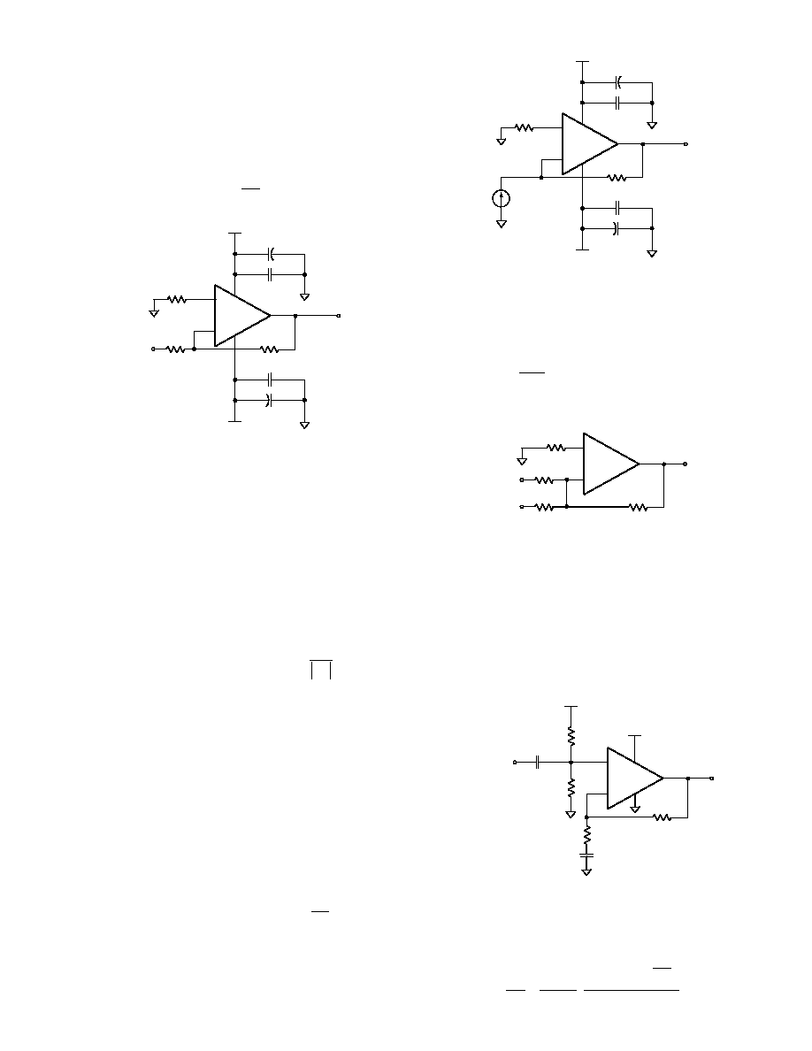
CLC446 Operation
The following topics will supply you with:
s
Design parameters, formulas and techniques
s
Interfaces
s
Application circuits
s
Layout techniques
s
SPICE model information
DC Gain (non-inverting)
The non-inverting DC voltage gain for the configuration
shown in Figure 1 is .
The normalized gain plots in the
Typical Performance
Characteristics
section show different feedback
resistors (R
f
) for different gains. These values of R
f
are
recommended for obtaining the highest bandwidth with
minimal peaking. The resistor R
t
provides DC bias for
the non-inverting input.
For A
v
< 5, use linear interpolation on the nearest A
v
val-
ues to calculate the recommended value of R
f
. For A
v
5, the minimum recommended R
f
is 200
.
Select R
g
to set the DC gain: .
DC gain accuracy is usually limited by the tolerance of R
f
and R
g
.
Figure 1: Non-Inverting Gain
+
-
CLC446
Fi
R
f
0.1
µ
F
6.8
µ
F
V
o
V
in
V
CC
0.1
µ
F
6.8
µ
F
V
EE
3
2
4
7
6
+
+
R
g
R
t
Typical Performance Characteristics
(V
CC
= ±5V, A
v
= +2, R
f
= 249
,,
R
L
= 100
; unless specified)
Short Term Settling Time
V
o
(% Output Step)
Time (sec)
0.2
0.1
-0.2
1n
10n
100n
0
-0.1
1
µ
10
µ
V
O
= 2V step
Long Term Settling Time
V
o
(% Output Step)
Time (s)
0.2
0.1
-0.2
1
µ
10
µ
100
µ
0
-0.1
1m
10m
100m
1
V
O
= 2V step
V
V
A
1
R
Z j
o
in
v
f
=
+
( )
Z j
R
f
( )
A
1
R
R
v
f
g
= +
R
R
A
1
g
f
v
=
-
CLC446 Design Information
5
http://www.national.com
DC Gain (unity gain buffer)
The recommended R
f
for unity gain buffers is 453
. R
g
is left open. Parasitic capacitance at the inverting node
may require a slight increase of R
f
to maintain a flat
frequency response.
DC Gain (inverting)
The inverting DC voltage gain for the configuration
shown in Figure 2 is .
Figure 2: Inverting Gain
The normalized gain plots in the
Typical Performance
Characteristics
section show different feedback
resistors (R
f
) for different gains. These values of R
f
are
recommended for obtaining the highest bandwidth with
minimal peaking. The resistor R
t
provides DC bias for the
non-inverting input.
For |A
v
| < 5, use linear interpolation on the nearest A
v
val-
ues to calculate the recommended value of R
f
. For |A
v
|
5, the minimum recommended R
f
is 200
.
Select R
g
to set the DC gain: . At large
gains, R
g
becomes small and will load the previous stage.
This can be solved by driving R
g
with a low impedance
buffer like the CLC111, or increasing R
f
and R
g
.
See the
AC Design (small signal bandwidth)
sub-section for the tradeoffs.
DC gain accuracy is usually limited by the tolerance of R
f
and R
g
.
DC Gain (transimpedance)
Figure 3 shows a transimpedance circuit where the cur-
rent I
in
is injected at the inverting node. The current
source's output resistance is much greater than R
f
.
The DC transimpedance gain is:
The recommended R
f
is 453
. Parasitic capacitance at
the inverting node may require a slight increase of R
f
to
maintain a flat frequency response.
DC gain accuracy is usually limited by the tolerance of R
f
.
Figure 3: Transimpedance Gain
DC Design (level shifting)
Figure 4 shows a DC level shifting circuit for inverting
gain configurations. V
ref
produces a DC output level
shift of , which is independent of the DC
output produced by V
in
.
Figure 4: Level Shifting Circuit
DC Design (single supply)
Figure 5 is a typical single-supply circuit. R
1
and R
2
form
a voltage divider that sets the non-inverting input DC volt-
age. This circuit has a DC gain of 1. A low
frequency zero is set by R
g
and C
2
. The coupling capac-
itor C
1
isolates its DC bias point from the
previous stage. Both capacitors make a high pass
response; high frequency gain is determined by R
f
and R
g
.
Figure 5: Single Supply Circuit
The complete gain equation for the circuit in Figure 5 is:
A
R
R
v
f
g
= -
+
-
CLC446
R
f
0.1
µ
F
6.8
µ
F
V
o
V
in
V
CC
0.1
µ
F
6.8
µ
F
V
EE
R
g
R
t
3
2
4
7
6
+
+
R
R
A
g
f
v
=
A
V
I
R
R
o
in
f
=
= -
+
-
CLC446
R
f
0.1
µ
F
6.8
µ
F
V
o
V
CC
0.1
µ
F
6.8
µ
F
V
EE
R
t
3
2
4
7
6
+
+
I
in
V
in
R
g
+
-
CLC446
R
f
V
o
V
ref
R
ref
R
t
+
-
CLC446
R
f
V
o
V
in
V
CC
R
g
R
2
R
1
V
CC
C
1
C
2
V
V
s
1 s
1 s
1
R
R
1 s
o
in
1
1
2
f
g
2
=
+
+
+
+
-
V
R
R
ref
f
ref