 | –≠–ª–µ–∫—Ç—Ä–æ–Ω–Ω—ã–π –∫–æ–º–ø–æ–Ω–µ–Ω—Ç: CLC449 | –°–∫–∞—á–∞—Ç—å:  PDF PDF  ZIP ZIP |
Features
s
1.1GHz small-signal bandwidth (A
v
= +2)
s
2500V/
µ
s slew rate
s
0.03%, 0.02∞ D
G
, D
s
6ns settling time to 0.2%
s
3rd order intercept, 30dBm @ 70MHz
s
Dual ±5V or single 10V supply
s
High output current: 90mA
s
2.5dB noise figure
Applications
s
High performance RGB video
s
RF/IF amplifier
s
Instrumentation
s
Medical electronics
s
Active filters
s
High-speed A/D driver
s
High-speed D/A buffer
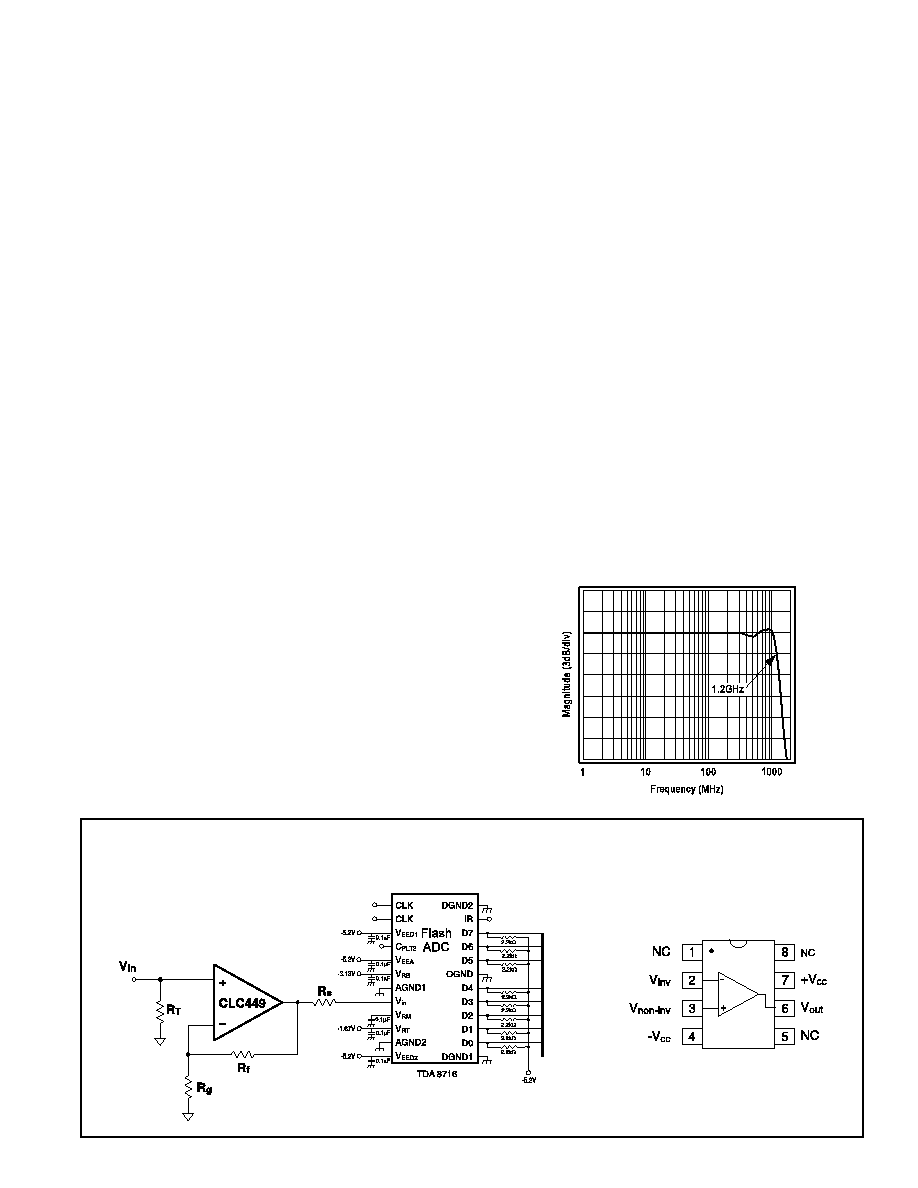
Typical Application
120MSPS High-Speed Flash ADC Driver
Pinout
DIP & SOIC
General Description
The CLC449 is an ultra-high-speed monolithic op amp, with a typ-
ical -3dB bandwidth of 1.1GHz at a gain of +2. This wideband op
amp supports rise and fall times less than 1ns, settling time of 6ns
(to 0.2%) and slew rate of 2500V/
µ
s. The CLC449 achieves 2nd
harmonic distortion of -68dBc at 5MHz at a low supply current of
only 12mA. These performance advantages have been achieved
through improvements in National's proven current feedback
topology combined with a high-speed complementary bipolar
process.
The DC to 1.2GHz bandwidth of the CLC449 is suitable for many IF
and RF applications as a versatile op amp building block for replace-
ment of AC coupled discrete designs. Operational amplifier
functions such as active filters, gain blocks, differentiation, addition,
subtraction and other signal conditioning functions take full
advantage of the CLC449's unity-gain stable closed-loop
performance.
The CLC449 performance provides greater headroom for lower
frequency applications such as component video, high-resolution
workstation graphics, and LCD displays. The amplifier's 0.1dB
gain flatness to beyond 200MHz, plus 0.8ns 2V rise and fall times
are ideal for improved time domain performance.
In
addition, the 0.03%/0.02∞ differential gain/phase performance
allows system flexibility for handling standard NTSC and PAL
signals.
In applications using high-speed flash A/D and D/A converters, the
CLC449 provides the necessary wide bandwidth (1.1GHz), settling
(6ns to 0.2%) and low distortion into 50
loads to improve SFDR.
Frequency Response (A
v
= +2V/V)
CLC449
1.1GHz Ultra-Wideband Monolithic Op Amp
N
June 1999
CLC449
1.1GHz Ultra-Wideband Monolithic Op Amp
© 1999 National Semiconductor Corporation
http://www.national.com
Printed in the U.S.A.
http://www.national.com
2
PARAMETERS
CONDITIONS TYP
MIN/MAX RATINGS
UNITS
NOTES
CLC449
+25∞
+25∞
0∞ to +70∞ -40∞ to +85∞
FREQUENCY DOMAIN RESPONSE
-3dB bandwidth
small signal
<0.2V
pp
1100
MHz
large signal
<2V
pp
500
380
380
360
MHz
±0.1 dB bandwidth
<2V
pp
200
MHz
gain flatness
peaking
DC to 200MHz
0
dB
rolloff
DC to 200MHz
0.1
0.5
0.5
0.5
dB
linear phase deviation
<200MHz
0.8
deg
differential gain
4.43MHz, R
L
=150
0.03
0.05
0.05
0.05
%
differential phase
4.43MHz, R
L
=150
0.02
0.02
0.05
0.05
deg
TIME DOMAIN RESPONSE
rise and fall time
2V step
0.8
1.1
1.1
1.1
ns
settling time to 0.2%
2V step
6
ns
settling time to 0.1%
2V step
11
ns
overshoot
2V step
10
18
18
18
%
slew rate
4V step
2500
2000
2000
2000
V/
µ
s
DISTORTION AND NOISE RESPONSE
2nd harmonic distortion
2V
pp
, 5MHz
-63
59
59
59
dBc
2V
pp
, 20MHz
-52
-48
-48
-48
dBc
2V
pp
, 50MHz
-44
40
40
40
dBc
3rd harmonic distortion
2V
pp
, 5MHz
-84
77
75
75
dBc
2V
pp
, 20MHz
-73
-66
-64
-64
dBc
2V
pp
, 50MHz
-62
55
53
53
dBc
3rd order intercept
70MHz
30
dBm
1dB gain compression @ 50MHz
16
dBm
equivalent input noise
non-inverting voltage
1MHz
2.2
2.9
nV/
Hz
inverting current
1MHz
15
20.0
pA/
Hz
non-inverting current
1MHz
3
5.0
pA/
Hz
STATIC DC PERFORMANCE
input offset voltage
3
7
9
9
mV
A
average drift
25
µ
V/∞C
input bias current
non-inverting
6
30
45
60
µ
A
A
average drift
50
nA/∞C
input bias current
inverting
2
20
25
40
µ
A
A
average drift
25
nA/∞C
power supply rejection ratio
DC
48
43
41
41
dB
A
common-mode rejection ratio
DC
47
44
45
46
dB
supply current
R
L
=
12
13.5
14
14
mA
A
MISCELLANEOUS PERFORMANCE
input resistance
non-inverting
400
200
200
150
k
input capacitance
non-inverting
1.3
pF
output resistance
closed loop
0.1
0.15
0.15
0.25
output voltage range
R
L
=
3.3
3.1
3.1
3.1
V
R
L
=100
2.9
2.8
2.8
2.8
V
input voltage range
common-mode
2.4
2.2
2.1
1.9
V
output current
80
60
50
40
mA
CLC449 Electrical Characteristics
(A
v
= +2, R
f
= 250
,,
V
cc
= ±5V, R
L
= 100
; unless specified)
Absolute Maximum Ratings
V
oc
±6V
I
out
is short circuit protected to ground
common-mode input voltage
±Vcc
maximum junction temperature
+150∞C
operating temperature range
AJ
-40∞C to +85∞C
storage temperature range
-65∞C to +150∞C
lead temperature (soldering 10 sec)
+300∞C
ESD (human body model)
500V
Notes
A) J-level: spec is 100% tested at +25∞C.
Package Thermal Resistance
Package
JC
JA
Plastic (AJP)
90∞C/W
105∞C/W
Surface Mount (AJE)
110∞C/W
130∞C/W
Min/max ratings are based on product characterization and simulation. Individual parameters are tested as noted. Outgoing quality levels are
determined from tested parameters.
3
http://www.national.com
10k
100k
1M
10M
100M
Magnitude (3dB/div)
20 log|Z| (dB
)
Distortion (dBc)
Noise Voltage (nV/
Hz), Current (pA/
Hz)
Frequency (Hz)
PSRR/CMRR (dB)
Magnitude (3dB/div)
Phase (deg)
Distortion (dBc)
Phase
(deg)
Distortion (dBc)
-3dB Bandwidth (MHz)
R
out
(ohms)
Time (1ns/div)
Time (1ns/div)
D.G. (%), D.P. (deg)
Magnitude (0.1dB/div)
Intercept Point (dBm)
Phase (deg)
Magnitude (3dB/div)
Phase (deg)
Phase (1deg/div)
PSRR
P
o
= 10dBm
100M
0.1M
1M
10M
0.1k
1k
10k
100k
1M
10M
100M
0.1M
1M
10M
100M
180
160
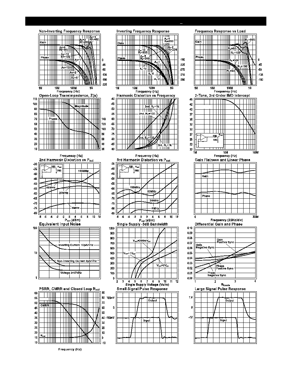
CLC449 Typical Performance Characteristics
(T
A
= 25∞C, V
cc
= + 5V, R
f
= 250
, A
v
= +2, R
L
= 100
)

http://www.national.com
4
CLC449 Typical Performance Characteristics
(T
A
= 25∞C, V
cc
= + 5V, R
f
= 250
, A
v
= +2, R
L
= 100
)
CLC449 OPERATION
Magnitude (1dB/div)
Input Offset Voltage, V
IO
(mV)
Input Bias Current, I
BI
, I
BN
(
µ
A)
Settling Time (ns)
R
s
(ohms)
VSWR
Frequency (Hz)
1.9
1.8
1.7
1.6
1.5
1.4
1.3
1.2
1.1
1.0
0.9
Input VSWR
Non-Inverting
Inverting
0
100M
200M
300M
400M
500M
VSWR
Frequency (Hz)
2.8
2.6
2.4
2.2
2.0
1.8
1.6
1.4
1.2
1.0
0.8
Uncompensated
Compensated
0
100M
200M
300M
400M
500M
|S
12
| (dB)
Frequency (Hz)
-10
-20
-30
-40
-50
-60
-70
-80
-90
-100
0
100M
200M
300M
400M
500M
Output VSWR
Reverse Isolation (S
12
)
Gain Compression
CLC449 Extended Application Information
The following design and application topics will supply
you with:
∑
A comprehensive set of design parameters and
design parameter adjustment techniques.
∑
A set of formulas that support design parameter
change prediction.
∑
A series of common applications that the CLC449
supports.
∑
A set of easy to use design guidelines for the
CLC449.
Additional design applications are possible with the
CLC449. If you have application questions, call 1-800-272-
9959 in the U.S. to contact a technical staff member.
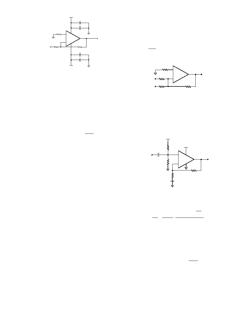
DC Gain (Non-Inverting)
The non-inverting DC voltage gain for the configuration
shown in Figure 1 is:
Figure 1: Non-Inverting Gain
The normalized gain plots in the
Typical Performance
Characteristics section show different feedback resistors,
R
f
, for different gains. These values of R
f
are recom-
mended for obtaining the highest bandwidth with minimal
peaking. The resistor R
t
in Figure 1 provides DC bias for
the non-inverting input.
For A
v
5, calculate the recommended R
f
as follows:
R
f
340 - A
v
∑
R
i
, where R
i
= 45
. For A
v
> 5, the
minimum recommended feedback resistor is R
f
= 100
.
Select R
g
to set the DC gain:
Accuracy of DC gain is usually limited by the tolerance of
the external resistors R
f
and R
g
.
DC Gain (Unity Gain Buffer)
Unity gain buffers are easily designed with a current-
feedback amplifier as long as the recommended feed-
back resistor R
f
= 402
is used and R
g
=
, i.e. open.
Parasitic capacitance at the inverting node may require a
slight increase of the feedback resistor R
f
to maintain a
flat frequency response.
DC Gain (Inverting)
The inverting DC voltage gain for the configuration shown
in Figure 2 is:
A
1
R
R
V
f
g
= +
+
-
CLC449
R
f
0.1
µ
F
6.8
µ
F
V
o
V
in
V
cc
R
g
R
t
3
2
4
7
6
+
0.1
µ
F
6.8
µ
F
V
ee
+
R
R
A
1
g
f
v
=
-
A
R
R
v
f
g
= -
5
http://www.national.com
Figure 2: Inverting Gain
The normalized gain plots in the
Typical Performance
Characteristics section show different feedback resistors,
R
f
, for different gains. These values of R
f
are recommended
for obtaining the highest bandwidth with minimal peaking.
The resistor R
t
in Figure 2 provides DC bias for the non-
inverting input.
For |Av|
4, calculate the recommended R
f
as follows:
Rf
295 - |A
v
|
∑
R
i
, where R
i
= 45
. For |A
v
| > 4, the
minimum recommended feedback resistor is R
f
= 100
.
Select R
g
to set the DC gain:
At large gains, R
g
becomes small and will load the
previous stage.
This situation is resolved by driving
R
g
with a low impedance buffer like the CLC111,
or increasing R
f
and R
g
(see the
Bandwidth (Small
Signal) sub-section for the tradeoffs).
Accurate DC gain is usually limited by the tolerance of
the external resistors R
f
and R
g
.
Bandwidth (Small Signal)
The CLC449 current-feedback amplifier bandwidth is a
function of the feedback resistor (R
f
), not of the DC volt-
age gain (A
v
).
The bandwidth is approximately
proportional to 1/R
f
. As a rule, if R
f
doubles, the band-
width is cut in half. Other AC specifications will also be
degraded.
Decreasing R
f
from the recommended
value increases peaking and for very small values of
R
f
oscillation will occur.
With an inverting amplifier design, peaking is sometimes
observed. This is often the result of layout parasitics
caused by inadequate ground planes or long traces. If
this is observed, placing a 50 to 200
resistor between
the non-inverting pin and ground will usually reduce the
peaking.
Bandwidth (Minimum Slew Rate)
Slew rate influences the bandwidth for large signal
sinusoids. To determine an approximate value of slew
rate, necessary to support large sinusoids use the
following equation:
SR
5
∑
f
∑
V
peak
V
peak
is the peak output sinusoidal voltage, f is the
frequency of the sinusoid.
The slew rate of the CLC449 in inverting gains is always
higher than in non-inverting gains.
DC Design (Level Shifting)
Figure 3 shows a DC level shifting circuit for inverting
gain configurations. V
ref
produces a DC output level shift
of
which is independent of the DC output produced by V
in
.
Figure 3: Level Shifting Circuit
DC Design (Single Supply)
Figure 4 is a typical single-supply circuit. Resistors R
1
and R
2
form a voltage divider that sets the non-inverting
input DC voltage. This circuit has a DC gain of 1. The
coupling capacitor C
1
isolates the DC bias point from the
previous stage.
Both capacitors make a high pass
response; the high frequency gain is determined by R
f
and R
g
.
Figure 4: Single Supply Circuit
The complete gain equation for the circuit in Figure 4 is:
where s = j
,
1
= (R
1
|| R
2
)
∑
C
1
, and
2
= R
g
C
2
.
DC Design (DC Offsets)
The DC offset model shown in Figure 5 is used to
calculate the output offset voltage. The equation for out-
put offset voltage is:
The current offset terms, I
BN
and I
BI
,
do not track each
other. The specifications are stated in terms of
magnitude only. Therefore, the terms V
os
, I
BN
, and I
BI
may have either positive or negative polarity. Matching
the equivalent resistance seen at both input pins does
not reduce the output offset voltage.
+
-
CLC449
R
f
0.1
µ
F
6.8
µ
F
V
o
V
in
V
cc
0.1
µ
F
6.8
µ
F
V
ee
R
g
R
t
3
2
4
7
6
+
+
R
R
| A |
g
f
v
=
-V
R
R
ref
f
ref
V
in
R
eq2
+
-
CLC449
R
f
V
o
V
ref
R
ref
R
eq1
+
-
CLC449
R
f
V
o
V
in
V
cc
R
g
R
2
R
1
V
cc
C
1
C
2
V
V
I
R
1
R
R
I
R
o
os
BN
eq1
f
eq2
BI
f
= -
+
(
)
+
+
(
)
V
V
s
1 s
1 s
1
R
R
1 s
o
in
1
1
2
f
g
2
=
+
+
+
+