 | –≠–ª–µ–∫—Ç—Ä–æ–Ω–Ω—ã–π –∫–æ–º–ø–æ–Ω–µ–Ω—Ç: CLC452AJP | –°–∫–∞—á–∞—Ç—å:  PDF PDF  ZIP ZIP |
CLC452
Single Supply, Low Power, High Output, Current
Feedback Amplifier
General Description
The CLC452 has a new output stage that delivers high
output drive current (100mA), but consumes minimal
quiescent supply current (3.0mA) from a single 5V supply. Its
current feedback architecture, fabricated in an advanced
complementary
bipolar
process,
maintains
consistent
performance over a wide range of gains and signal levels,
and has a linear-phase response up to one half of the -3dB
frequency.
The CLC452 offers superior dynamic performance with a
130MHz small signal bandwidth, 400V/µs slew rate and
4.5ns rise/fall times (2V
STEP
. The combination of low
quiescent power, high output current drive, and high speed
performance make the CLC452 well suited for many battery
powered personal communication/computing systems.
The ability to drive low impedance, high capacitive loads,
makes the CLC452 ideal for single ended cable applications.
It also drives low impedance loads with minimum distortion.
The CLC452 will drive a 100
load with only -75/-74dBc
second/third harmonic distortion (A
V
= +2, V
OUT
= 2V
PP
, f
=1MHz). With a 25
load, and the same conditions, it
produces only -65/-77dBc second/third harmonic distortion.
It is also optimized for driving high currents into single-ended
transformers and coils.
When driving the input of high resolution A/D converters, the
CLC452
provides
excellent
-78/-85dBc
second/third
harmonic distortion (A
V
= +2, V
OUT
= 2V
PP
, f =1MHz, R
L
=
1k
) and fast settling time.
Available in SOT23-5, the CLC452 is ideal for applications
where space is critical.
Features
n
100mA output current
n
3.0mA supply current
n
130MHz bandwidth (A
V
= +2)
n
-78/-85dBc HD2/HD3 (1MHz)
n
25ns settling to 0.05%
n
400V/µs slew rate
n
Stable for capacitive loads up to 1000pF
n
Single 5V to
±
5V supplies
n
Available in Tiny SOT23-5 package
Applications
n
Coaxial cable driver
n
Twisted pair driver
n
Transformer/Coil Driver
n
High capacitive load driver
n
Video line driver
n
Portable/battery powered applications
n
A/D driver
Connection Diagrams
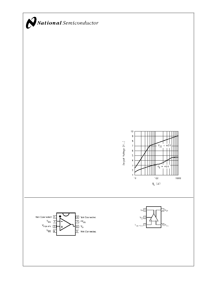
Maximum Output Voltage vs. R
L
DS012790-1
DS012790-5
Pinout
DIP & SOIC
DS012790-4
Pinout
SOT23-5
March 2001
CLC452
Single
Supply
,
Low
Power
,
High
Output,
Current
Feedback
Amplifier
© 2001 National Semiconductor Corporation
DS012790
www.national.com

Typical Application
Ordering Information
Package
Temperature Range
Industrial
Part Number
Package Marking
NSC Drawing
8-pin plastic DIP
-40∞C to +85∞C
CLC452AJP
CLC452AJP
N08E
8-pin plastic SOIC
-40∞C to +85∞C
CLC452AJE
CLC452AJE
M08A
5-pin SOT
-40∞C to +85∞C
CLC452AJM5
A21
MA05A
DS012790-2
Single Supply Cable Driver
DS012790-3
Response After 10m of Cable
CLC452
www.national.com
2
Absolute Maximum Ratings
(Note 1)
If Military/Aerospace specified devices are required,
please contact the National Semiconductor Sales
Office/Distributors for availability and specifications.
Supply Voltage (V
CC
-(V
EE
)
+14V
Output Current (see note 3)
140mA
Common Mode Input Voltage
V
EE
to V
CC
Maximum Junction Temperature
+150∞C
Storage Operating Temperature
Range
-65∞C to +150∞C
Lead Solder Duration (+300∞C)
10 sec
ESD Rating (human body model)
500V
Operating Ratings
Thermal Resistance
Package
(
JC
)
(
JA
)
MDIP
105∞C/W
155∞C/W
SOIC
95∞C/W
175∞C/W
SOT23
140∞C/W
210∞C/W
+5V Electrical Characteristics
A
V
= +2, V
S
= +5V(Note 5), V
CM
= V
EE
+ (V
S
/2), R
L
= 100
, R
f
= 1k
, R
L
tied to V
CM
; unless specified
Symbol
Parameter
Conditions
Typ
Min/Max (Note 2)
Units
Ambient Temperature
CLC452AJ
+25∞C
+25∞C
0 to
70∞C
-40 to
85∞C
Frequency Domain Response
-3dB Bandwidth
V
O
<
0.5V
PP
130
95
90
85
MHz
V
O
<
2.0V
PP
95
80
77
75
MHz
-0.1dB Bandwidth
V
O
<
0.5V
PP
30
25
20
20
MHz
Gain Peaking
<
200MHz, V
O
<
0.5V
PP
0
0.5
0.9
1.0
dB
Gain Rolloff
<
30MHz V
O
<
0.5V
PP
0.1
0.3
0.3
0.3
dB
linear phase deviation
<
30MHz, V
O
= 0.5V
PP
0.1
0.2
0.3
0.3
deg
TIME DOMAIN RESPONSE
Rise and Fall Time
2V Step
4.5
6.0
6.4
6.8
ns
Settling Time to
±
0.05%
1V Step
25
-
-
-
ns
Overshoot
2V Step
11
15
18
18
%
Slew Rate
2V Step
400
300
275
260
V/µs
DISTORTION AND NOISE RESPONSE
2nd Harmonic Distortion
2V
PP
, 1MHz
-75
-69
-67
-67
dBc
2V
PP
,1MHz R
L
= 1k
-78
-70
-68
-68
dBc
2V
PP
, 5MHz
-65
-58
-56
-56
dBc
3rd Harmonic Distortion
2V
PP
, 1MHz
-74
-70
-68
-68
dBc
2V
PP
, 1MHz R
L
=1k
-85
-75
-73
-73
dBc
2V
PP
, 5MHz
-60
-55
-53
-53
dBc
Equivalent Input Noise
Voltage (e
ni
)
>
1MHz
2.8
3.5
3.8
3.8
nV/
Non-Inverting Current (i
bn
)
>
1MHz
7.5
10
11
11
pA/
Non-Inverting Current (i
bi
)
>
1MHz
10.5
14
15
15
pA/
Static, DC Performance
Input Offset Voltage (Note 4)
1
4
6
6
mV
Average Drift
8
-
-
-
µV/∞C
Input Bias Current
(non-inverting) (Note 4)
6
18
22
24
µA
Average Drift
40
-
-
-
nA/∞C
Input Bias Current (inverting)
(Note 4)
6
14
16
17
µA
Average Drift
25
-
-
-
nA/∞C
Power Supply Rejection Ratio
DC
48
45
43
43
dB
Common-Mode Rejection Ratio
DC
51
48
46
46
dB
CLC452
www.national.com
3

+5V Electrical Characteristics
(Continued)
A
V
= +2, V
S
= +5V(Note 5), V
CM
= V
EE
+ (V
S
/2), R
L
= 100
, R
f
= 1k
, R
L
tied to V
CM
; unless specified
Symbol
Parameter
Conditions
Typ
Min/Max (Note 2)
Units
Static, DC Performance
Supply Current (Note 4)
R
L
=
3.0
3.4
3.6
3.6
mA
Miscellaneous Performance
Input Resistance (non-inverting)
0.39
0.28
0.25
0.25
M
Input Capacitance
(non-inverting)
1.5
2.3
2.3
2.3
pF
Input Voltage Range, High
4.2
4.1
4.0
4.0
V
Input Voltage Range, Low
0.8
0.9
1.0
1.0
V
Output Voltage Range, High
R
L
= 100
4.0
3.9
3.8
3.8
V
Output Voltage Range, Low
R
L
= 100
1.0
1.1
1.2
1.2
V
Output Voltage Range, High
R
L
=
4.1
4.0
4.0
3.9
V
Output Voltage Range, Low
R
L
=
0.9
1.0
1.0
1.1
V
Output Current (Note 3)
100
80
65
40
mA
Output Resistance, Closed Loop
DC
70
105
105
140
m
±
5V Electrical Characteristics
A
V
= +2, V
CC
=
±
5V, R
L
=100
, R
f
= 1k
; unless specified
Symbol
Parameter
Conditions
Typ
Min/Max(Note 2)
Units
Ambient Temperature
CLC452AJ
+25∞C
+25∞C
0 to
70∞C
-40 to
85∞C
Frequency Domain Response
-3dB Bandwidth
V
O
<
1.0V
PP
160
135
120
115
MHz
V
O
<
4.0V
PP
75
60
57
55
MHz
-0.1dB Bandwidth
V
O
<
1.0V
PP
30
25
25
20
MHz
Gain Peaking
<
200MHz, V
O
<
1.0V
PP
0
0.5
0.9
1.0
dB
Gain Rolloff
<
30MHz, V
O
<
1.0V
PP
0.1
0.2
0.3
0.3
dB
Linear Phase Deviation
<
30MHz, V
O
<
1.0V
PP
)
0.1
0.2
0.3
0.3
deg
Differential Gain
NTSC, R
L
= 150
0.05
-
-
-
%
Differential Phase
NTSC, R
L
= 150
0.08
-
-
-
deg
TIME DOMAIN RESPONSE
Rise and Fall Time
2V Step
3.2
4.2
4.5
5.0
ns
Settling Time to
±
0.05%
2V Step
20
-
-
-
ns
Overshoot
2V Step
8
12
15
15
%
Slew Rate
2V Step
540
400
370
350
V/µs
DISTORTION AND NOISE RESPONSE
2nd Harmonic Distortion
2V
PP
,1MHz
-77
-71
-69
-69
dBc
2V
PP
,1MHz, R
L
= 1k
-78
-72
-70
-70
dBc
2V
PP
,5MHz
-69
-63
-61
-61
dBc
3rd Harmonic Distortion
2V
PP
, 1MHz
-72
-68
-66
-66
dBc
2V
PP
, 1MHz, R
L
= 1k
-90
-80
-78
-78
dBc
2V
PP
, 5MHz
-58
-54
-52
-52
dBc
Equivalent Input Noise
Voltage (e
ni
)
>
1MHz
2.8
3.5
3.8
3.8
nV/
Non-Inverting current (i
bn
)
>
1MHz
7.5
10
11
11
pA/
Inverting Current (i
bi
)
>
1MHz
10.5
14
15
15
pA/
CLC452
www.national.com
4
±
5V Electrical Characteristics
(Continued)
A
V
= +2, V
CC
=
±
5V, R
L
=100
, R
f
= 1k
; unless specified
Symbol
Parameter
Conditions
Typ
Min/Max(Note 2)
Units
Static, DC Performance
Input Offset Voltage
1
6
8
8
mV
Average Drift
10
-
-
-
µV/∞C
Input Bias Current
(non-inverting)
3
18
23
25
µA
Average Drift
40
-
-
-
nA/∞C
Input Bias Current (inverting)
13
24
31
31
µA
Average Drift
30
-
-
-
nA/∞C
Power Supply Rejection Ratio
DC
48
45
43
43
dB
Common-Mode Rejection Ratio
DC
53
50
48
48
dB
Supply Current
R
L
=
3.2
3.8
4.0
4.0
mA
Miscellaneous Performance
Input Resistance (non-inverting)
0.52
0.35
0.30
0.30
M
Input Capacitance
(non-inverting)
1.2
1.8
1.8
1.8
pF
Common-Mode Input Range
±
4.2
±
4.1
±
4.1
±
4.0
V
Output Voltage Range
R
L
= 100
±
3.8
±
3.6
±
3.6
±
3.5
V
Output Voltage Range
R
L
=
±
4.0
±
3.8
±
3.8
±
3.7
V
Output Current (Note 3)
130
100
80
50
mA
Output Resistance, Closed Loop
DC
60
90
90
120
m
Note 1: "Absolute Maximum Ratings" are those values beyond which the safety of the device cannot be guaranteed. They are not meant to imply that the devices
should be operated at these limits. The table of "Electrical Characteristics" specifies conditions of device operation.
Note 2: Min/max ratings are based on product characterization and simulation. Individual parameters are tested as noted. Outgoing quality levels are determined
from tested parameters.
Note 3: The short circuit current can exceed the maximum safe output current.
Note 4: AJ-level: spec. is 100% tested at +25∞C.
Note 5: V
S
= V
CC
- V
EE
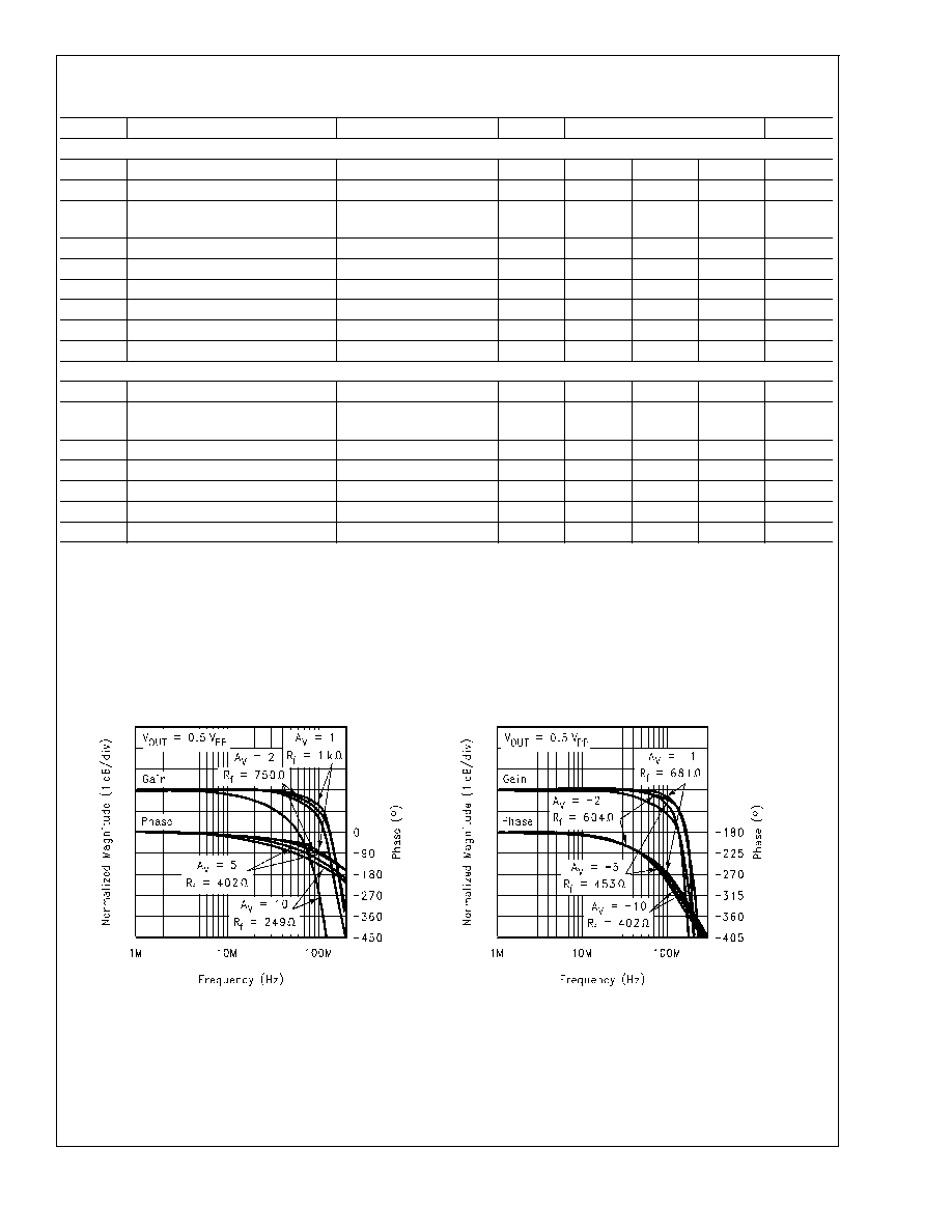
+5V Typical Performance Characteristics
Non-Inverting Frequency Response
DS012790-6
Inverting Frequency Response
DS012790-7
CLC452
www.national.com
5