Features
s
Output clamping with fast recovery
s
0.0025% settling in 25ns (32ns max.)
s
Low power, 170mW
s
Low distortion. -50dBc at 20MHz
Applications
s
Output clamping applications
s
High-accuracy A/D systems (12-14 bits)
s
High-accuracy D/A converters
s
Pulse amplitude modulation systems
General Description
CLC502
Clamping, Low-Gain Op Amp with Fast 14-bit Settling
N
June 1999
CLC502
Clamping,
Lo
w-Gain Op Amp with F
ast 14-bit Settling
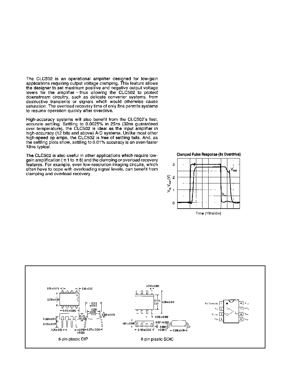
Package Dimensions
Pinout
DIP & SOIC
© 1999 National Semiconductor Corporation
http://www.national.com
Printed in the U.S.A.
The CLC502 is available in several versions to meet a variety of
requirements. A three-letter suffix determines the version:
CLC502AJP
-40∞C to +85∞C
8-pin plastic DIP
CLC502AJE
-40∞C to +85∞C
8-pin plastic SOIC
DESC SMD number: 5962-91743
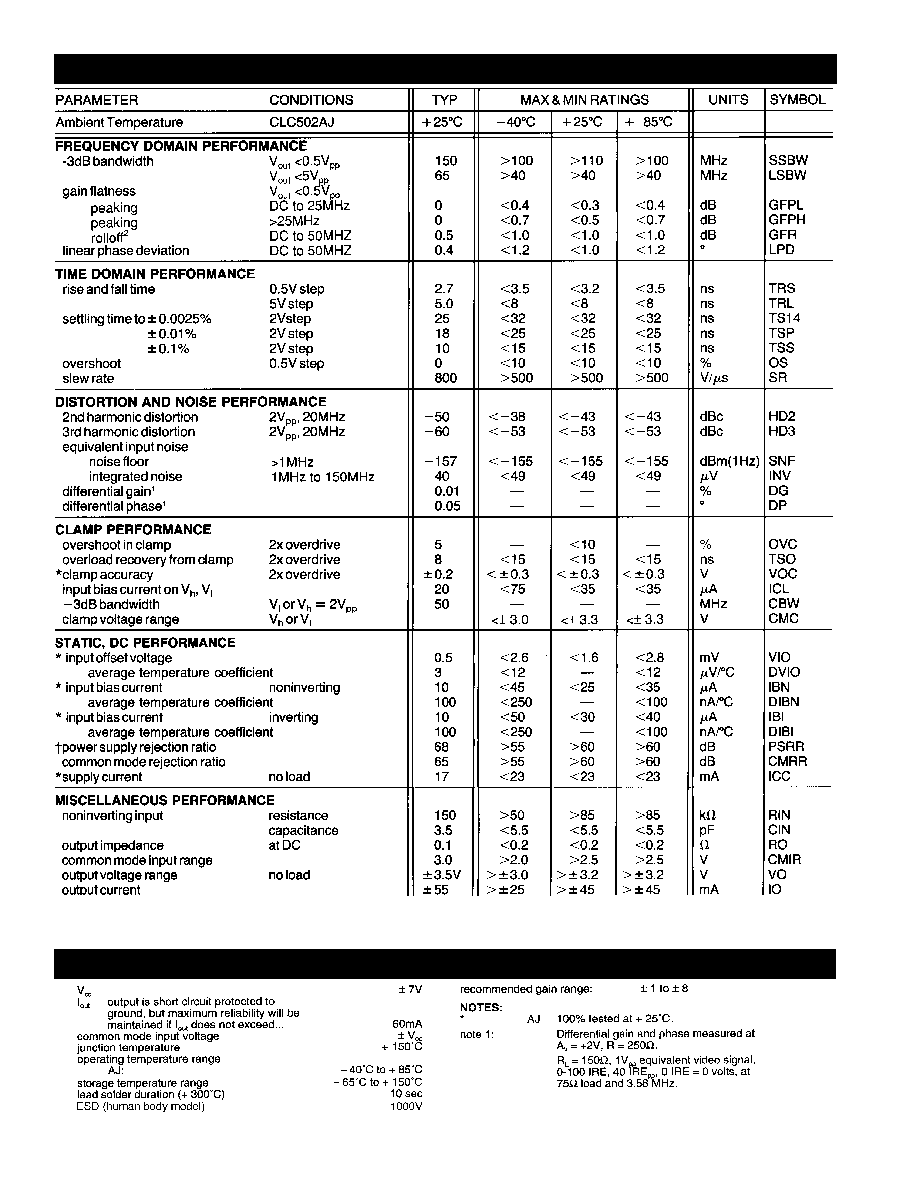
CLC502 Electrical Characteristics
(A
v
= +2,V
cc
= ±5V, R
L
= 100
, R
f
= 250
,V
H
= +3V
,
V
L
= -3V)
Absolute Maximum Ratings
Miscellaneous Ratings
http://www.national.com
2
Min/max ratings are based on product characterization and simulation. Individual parameters are tested as noted. Outgoing quality levels are
determined from tested parameters.
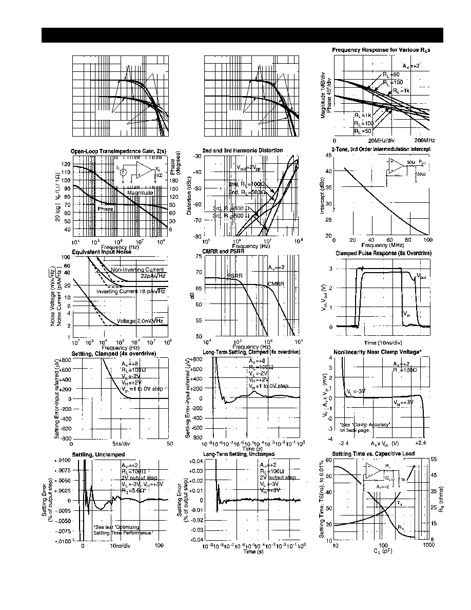
Typical Performance Characteristics
(T
A
= 25∞, A
v
= +2, V
CC
= ±5V, R
L
= 100
,,
R
f
= 250
, V
H
= +3V, V
L
= -3V )
Non-Inverting Frequency Response
Magnitude (1dB/div)
1
10
100
Phase (deg)
-180
-450
-270
-360
-90
0
V
out
= 0.5V
pp
A
v
= 2
R
f
= 249
A
v
= 1
R
f
= 301
A
v
= 8
R
f
= 110
A
v
= 4
R
f
= 200
Frequency (MHz)
Inverting Frequency Response
Magnitude (1dB/div)
1
10
100
Phase (deg)
-360
-630
-450
-540
-270
-180
V
out
= 0.5V
pp
A
v
= -2
R
f
= 237
A
v
= -1
R
f
= 249
A
v
= -8
R
f
= 210
A
v
= -4
R
f
= 249
Frequency (MHz)
3
http://www.national.com