Äîêóìåíòàöèÿ è îïèñàíèÿ www.docs.chipfind.ru
D
P
8382
1 10/1
00/10
00 Mb
/s P
C
I E
t
h
e
r
n
et
N
e
two
r
k
Inte
r
f
ace C
o
nt
r
o
ller
©
2001 National Semiconductor Corporation
www.national.com
PRELIMINARY
February 2001
DP83821
10/100/1000 Mb/s PCI Ethernet Network Interface
Controller
General Description
DP83821 is a single-chip 10/100/1000 Mb/s Ethernet
Controller for the PCI bus. It is targeted at high-
performance adapter cards and mother boards. The
DP83821 fully implements the V2.2 33 MHz, 32-bit PCI bus
interface for host communications with power management
support. Packet descriptors and data are transferred via
bus-mastering, reducing the burden on the host CPU. The
DP83821 can support full duplex 10/100/1000 Mb/s
transmission and reception.
Features
-- IEEE 802.3 Compliant, 33 Mhz, 32-bit PCI V2.2
MAC/BIU supports data rates from 1 Mb/s to 1000 Mb/s.
This allows support for traditional 10 Mb/s Ethernet, 100
Mb/s Fast Ethernet, as well as 1000 Mb/s Gigabit
Ethernet.
-- Flexible, programmable Bus master - burst sizes of up to
256 dwords (1024 bytes)
-- BIU compliant with PC 97 and PC 98 Hardware Design
Guides, PC 99 Hardware Design Guide draft, ACPI v1.0,
PCI Power Management Specification v1, OnNow
Device Class Power Management Reference
Specification - Network Device Class v1.0a
-- Wake on LAN (WOL) support compliant with PC98,
PC99, and OnNow, including directed packets, Magic
Packet with SecureOn, ARP packets, pattern match
packets, and Phy status change
-- GMII/MII provides IEEE 802.3 standard interface to
support 10/100/1000 Mb/s physical layer devices
-- Ten-Bit Interface (TBI) for support of 1000BASE-X
-- Virtual LAN (VLAN) and long frame support. VLAN tag
insertion support for transmit packets. VLAN tag
detection and removal for receive packets
-- 802.3x Full duplex flow control, including automatic
transmission of Pause frames based on Rx FIFO
thresholds
-- IPv.4 checksum task off-loading. Supports checksum
generation and verification of IP, TCP, and UDP headers
-- 802.1D and 802.1Q priority queueing support. Supports
multiple priority queues in both transmit and receive
directions.
-- Extremely flexible Rx packet filtration including: single
address perfect filter with MSb masking, broadcast,
2,048 entry multicast/unicast hash table, deep packet
pattern matching for up to 4 unique patterns.
-- Statistics gathered for support of RFC 1213 (MIB II),
RFC 1398 (Ether-like MIB), IEEE 802.3 LME, reducing
CPU overhead for management.
-- Internal 8 KB Transmit and 32 KB Receive data FIFOs
-- Supports Jumbo packets
-- Serial EEPROM port with auto-load of configuration data
from EEPROM at power-on
-- Flash/PROM interface for remote boot support
-- Full Duplex support for 10/100/1000 Mb/s data rates
-- 208-pin PQFP package
-- Low power CMOS design
-- 3.3V powered I/Os with 5V tolerant inputs
-- JTAG Boundary Scan supported
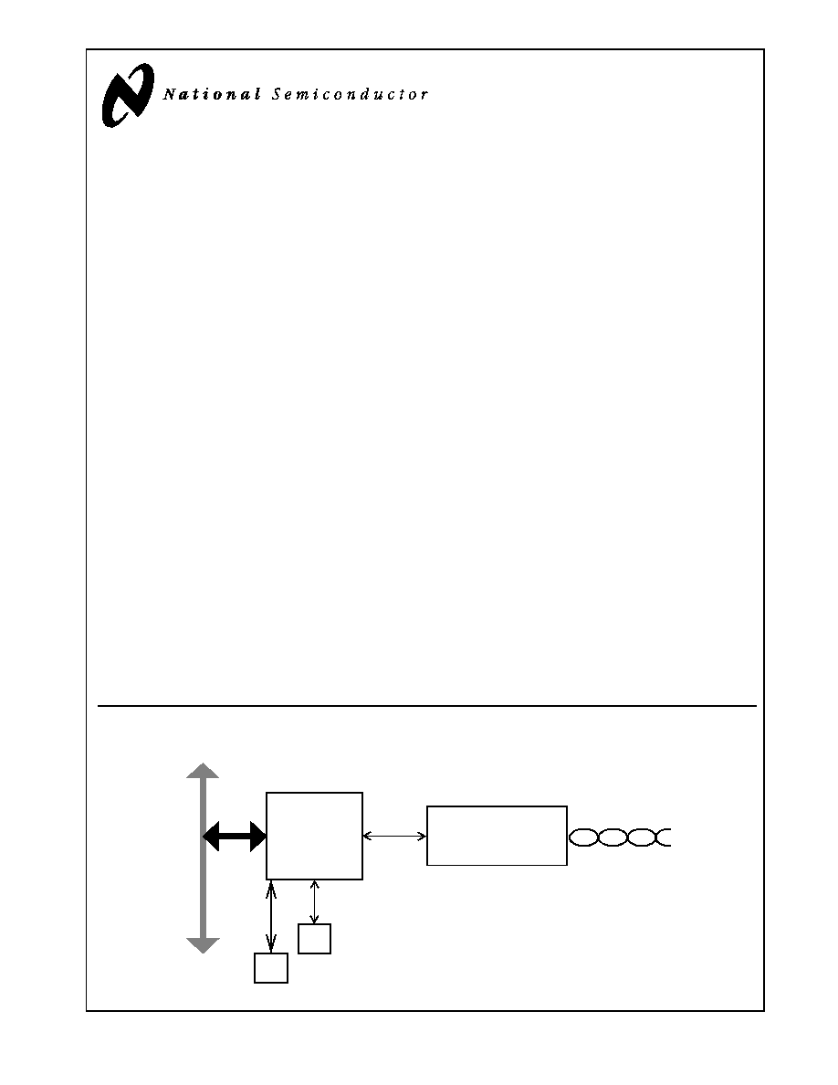
System Diagram
P C I B u s
D P 8 3 8 2 1
E E P R O M (o p tio n a l)
1 0 /1 0 0 /1 0 0 0 M b /s
PH Y
B o o t R O M (o p tio n a l)
M II
G M II
2
www.national.com
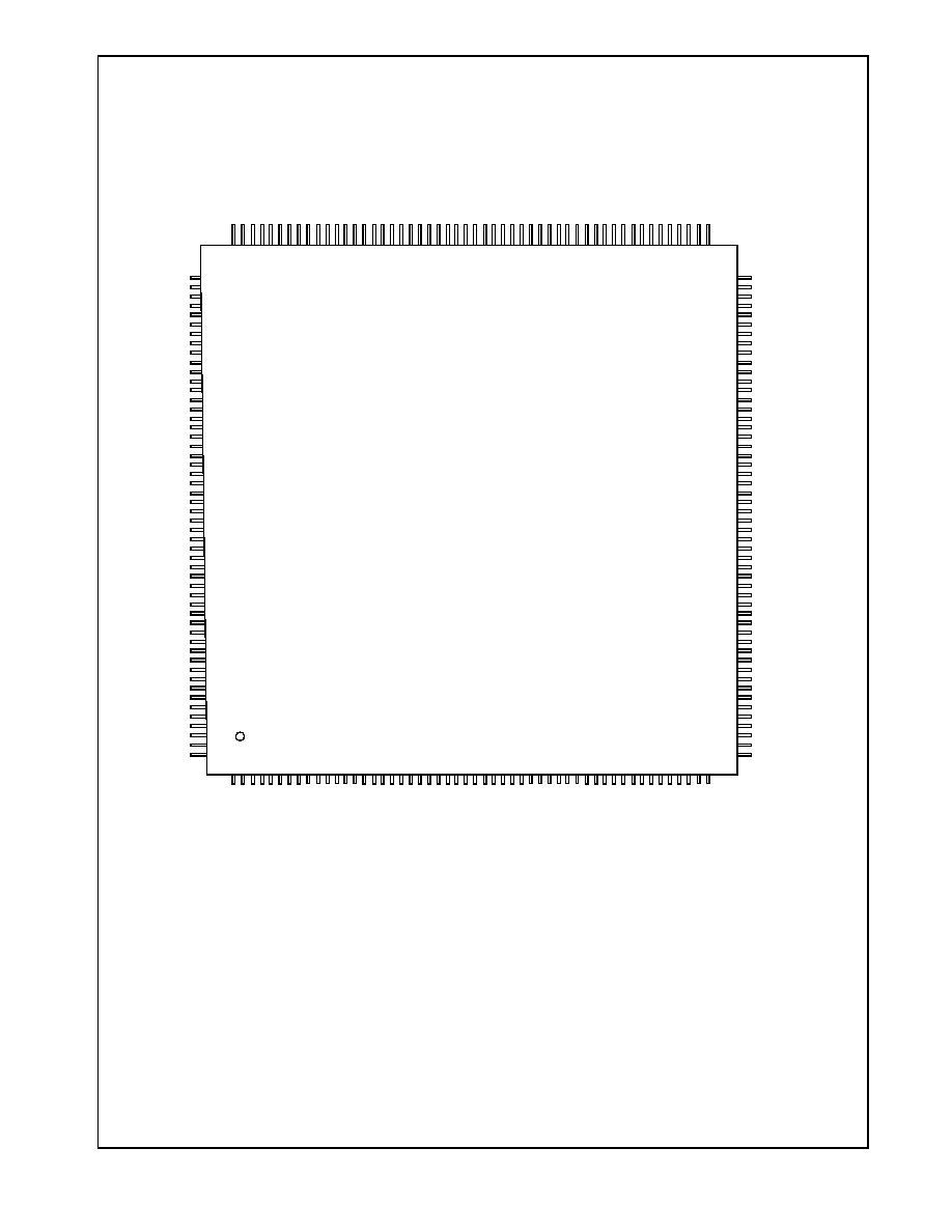
1.0 Connection Diagram
Order Number DP83821VUW
See NS Package Number NVUW208A
AD
1
6
CB
E
N
2
P
C
I
VSS
F
R
AM
EN
IRDY
N
T
RDY
N
PC
I
V
D
D
D
E
VSE
L
N
ST
O
P
N
P
E
RRN
S
E
RRN
PA
R
CB
E
N
1
AD
1
5
AD
1
4
P
C
I
VSS
AD
1
3
AD
1
2
AD
1
1
PC
I
V
D
D
AD
1
0
AD
9
AD
8
CB
E
N
0
AD
7
AD
6
P
C
I
VSS
AD
5
AD
4
PC
I
V
D
D
AD
3
AD
2
AD
1
AD
0
S
PEC
I
A
L
H
I
P
C
I
VSS
S
PEC
I
A
L
H
I
SPE
C
I
AL
L
O
SPE
C
I
AL
L
O
PC
I
V
D
D
SPE
C
I
AL
L
O
SPE
C
I
AL
L
O
SPE
C
I
AL
L
O
SPE
C
I
AL
L
O
SPE
C
I
AL
L
O
P
C
I
VSS
SPE
C
I
AL
L
O
SPE
C
I
AL
L
O
SPE
C
I
AL
L
O
SPE
C
I
AL
L
O
SPE
C
I
AL
L
O
P
C
IV
DDD
MD7
MD6
MD5
MD4/EEDO
VDDIO
VSSIO
MD3
MD2
MD1/CFGDISN
MD0/PMGDISN
MWRN
MRDN
MCSN
EESEL
RESERVED
COREVDD
COREVSS
CLKRUNN
3VAUX
PWRGOOD
PCIVIO
SPECIALLO
SPECIALLO
SPECIALLO
PCIVDD
SPECIALLO
SPECIALLO
SPECIALLO
PCIVSS
SPECIALLO
SPECIALLO
SPECIALLO
SPECIALLO
PCIVDD
SPECIALLO
SPECIALLO
SPECIALLO
SPECIALLO
PCIVSS
SPECIALLO
SPECIALLO
SPECIALLO
SPECIALLO
SPECIALLO
PCIVDD
SPECIALLO
SPECIALLO
SPECIALLO
PCIVSS
SPECIALLO
SPECIALLO
SPECIALLO
RXD0
RXD1
RXD2
RXD3
VSSIO
VDDIO
RXD4
RXD5
RXD6
RXD7
RXDV/RXD8
RXER/RXD9
CRS/SIG_DET
COL
RXEN
PHYRSTN
COREVSS
COREVDD
PMEN
PCICLK
TRSTN
TCK
TMS
TDO
TDI
PCIVSS
INTAN
RSTN
GNTN
REQN
PCIVDD
AD31
AD30
AD29
AD28
AD27
AD26
AD25
AD24
PCIVSS
CBEN3
IDSEL
AD23
AD22
PCIVDD
AD21
AD20
AD19
COREVSS
COREVDD
AD18
AD17
157
158
159
160
161
162
163
164
165
166
167
168
169
170
171
172
173
174
175
176
177
178
179
180
181
182
183
184
185
186
187
188
189
190
191
192
193
194
195
196
197
198
199
200
201
202
203
204
205
206
207
208
1
2
3
4
5
6
7
8
9
10
11
12
13
14
15
16
17
18
19
20
21
22
23
24
25
26
27
28
29
30
31
32
33
34
35
36
37
38
39
40
41
42
43
44
45
46
47
48
49
50
51
52
104
103
102
101
100
99
98
97
96
95
94
93
92
91
90
89
88
87
86
85
84
83
82
81
80
79
78
77
76
75
74
73
72
71
70
69
68
67
66
65
64
63
62
61
60
59
58
57
56
55
54
53
15
6
15
5
15
4
15
3
15
2
15
1
15
0
14
9
14
8
14
7
14
6
14
5
14
4
14
3
14
2
14
1
14
0
13
9
13
8
13
7
13
6
13
5
13
4
13
3
13
2
13
1
13
0
12
9
12
8
12
7
12
6
12
5
12
4
12
3
12
2
12
1
12
0
11
9
11
8
11
7
11
6
11
5
11
4
11
3
11
2
11
1
11
0
10
9
10
8
10
7
10
6
10
5
DP83821
Gigabit NIC
RX
CL
K
/
RX
P
M
A
C
L
K
1
T
X
CL
K
/
RX
P
M
A
C
L
K
0
T
XER
/
T
XD
9
T
XEN
/
T
XD
8
TX
D
7
/
M
A
1
5
TX
D
6
/
M
A
1
4
V
DDIO
VS
SI
O
TX
D
5
/
M
A
1
3
TX
D
4
/
M
A
1
2
TX
D
3
/
M
A
1
1
TX
D
2
/
M
A
1
0
V
DDIO
VS
SI
O
TX
D
1
/
M
A
9
TX
D
0
/
M
A
8
G
T
X
C
L
K
/
T
XPM
AC
L
K
MD
IO
MD
C
R
E
F
125
V
DDIO
VS
SI
O
S
P
D
1000
S
P
D
100
PH
Y
L
N
K
G
P
1
DUP
GP
5
GP
4
GP
3
GP
2
RE
S
E
RV
E
D
AV
D
D
AV
SS
O
S
CV
DD
X1
X2
O
S
C
VSS
RE
S
E
RV
E
D
RE
S
E
RV
E
D
RE
S
E
RV
E
D
CO
RE
V
D
D
CO
RE
V
S
S
MA
7
MA
6
MA
5
V
DDIO
VS
SI
O
M
A
4
/
EEC
L
K
M
A
3
/
EED
I
MA
2
MA
1
MA
0

3
www.national.com
2.0 Pin Descriptions
PCI Interface
Symbol
Pin No(s)
Direction
Description
AD31-0
188, 189, 190,
191, 192, 193,
194, 195, 199,
200, 202, 203,
204, 207, 208,
1, 14, 15, 17,
18, 19, 21, 22,
23, 25, 26, 28,
29, 31, 32, 33,
34
I/O
Address and Data: Multiplexed address and data bus. As a bus master, the
DP83821 will drive address during the first bus phase. During subsequent
phases, the DP83821 will either read or write data expecting the target to
increment its address pointer. As a bus target, the DP83821 will decode each
address on the bus and respond if it is the target being addressed.
CBEN3-0
197, 2, 13, 24
I/O
Bus Command/Byte Enable: During the address phase these signals define
the "bus command" or the type of bus transaction that will take place. During
the data phase these pins indicate which byte lanes contain valid data. CBEN0
applies to byte 0 (bits 7-0) and CBEN3 applies to byte 3(bits 31-24).
PCICLK
176
I
Clock: This PCI Bus clock provides timing for all bus phases. The rising edge
defines the start of each phase. The clock frequency ranges from 0 to 33 MHz.
DEVSELN
8
I/O
Device Select: As a target, the DP83821 asserts this signal low when it
recognizes its address after FRAMEN is asserted. As a bus master, the
DP83821 samples this signal to insure that the destination address for the data
transfer is recognized by a PCI target.
FRAMEN
4
I/O
Frame: As a bus master, this signal is asserted low to indicate the beginning
and duration of a bus transaction. Data transfer takes place when this signal is
asserted. It is de-asserted before the transaction is in its final phase. As a
target, the device monitors this signal before decoding the address to check if
the current transaction is addressed to it.
GNTN
185
I
Grant: This signal is asserted low to indicate to the DP83821 that it has been
granted ownership of the bus by the central arbiter. This input is used when the
DP83821 is acting as a bus master.
IDSEL
198
I
Initialization Device Select: This pin is sampled by the DP83821 to identify
when configuration read and write accesses are intended for it.
INTAN
183
O
Interrupt A: This signal is asserted low when an interrupt condition as defined
in the Interrupt Status Register, Interrupt Mask, and Interrupt Enable registers
occurs.
IRDYN
5
I/O
Initiator Ready: As a bus master, this signal will be asserted low when the
DP83821 is ready to complete the current data phase transaction. This signal is
used in conjunction with the TRYDN signal. Data transaction takes place at the
rising edge of PCICLK when both IRDYN and TRDYN are asserted low. As a
target, this signal indicates that the master has put the data on the bus.
PAR
12
I/O
Parity: This signal indicates even parity across AD31-0 and CBEN3-0 including
the PAR pin. As a master, PAR is asserted during address and write data
phases. As a target, PAR is asserted during read data phases.
PERRN
10
I/O
Parity Error: The DP83821 as a master or target will assert this signal low to
indicate a parity error on any incoming data (except for special cycles). As a
bus master, it will monitor this signal on all write operations (except for special
cycles).
REQN
186
O
Request: The DP83821 will assert this signal low to request the ownership of
the bus to the central arbiter.
RSTN
184
I
Reset: When this signal is asserted all outputs of DP83821 will be tri-stated
and the device will be put into a known state.

4
www.national.com
2.0 Pin Descriptions
(Continued)
SERRN
11
I/O
System Error: This signal is asserted low by DP83821 during address parity
errors and system errors if enabled.
STOPN
9
I/O
Stop: This signal is asserted low by the target device to request the master
device to stop the current transaction.
TRDYN
6
I/O
Target Ready: As a target, this signal will be asserted low when the (slave)
device is ready to complete the current data phase transaction. This signal is
used in conjunction with the IRDYN signal. Data transaction takes place at the
rising edge of PCICLK when both IRDYN and TRDYN are asserted low. As a
master, this signal indicates that the target is ready for the data during write
operation and with the data during read operation.
PMEN
175
O
Power Management Event: This signal is asserted low by DP83821 to
indicate that a power management event has occurred.
3VAUX
86
I
PCI Aux Voltage Sense: This pin is used to sense the presence of a 3.3v
auxiliary supply in order to define the PME Support available.
This pin pad has an internal weak pull down.
PWRGOOD
85
I
PCI bus power good: Connected to PCI bus 3.3v power, this pin is used to
sense the presence of PCI bus power during the D3 power management state.
This pin pad has an internal weak pull down.
CLKRUNN
87
I/O
Clockrun: This signal is asserted low by DP83821 to indicate that a Clockrun
Event has occurred.
PCIVIO
84
I
PCI Bus VIO: This pin should be connected to the VIO pins of the PCI bus. It
provides a direct connection to the ESDPLUS ring for biasing. It may be
connected to 5V if available. It should not be connected to 3.3V unless all
signaling is 3.3V as this will interfere with 5V tolerance. Care should be taken in
connecting this to power supplies when power management functions are
enabled.
Media Independent Interface (MII) - and Gigabit Media Independent Interface (GMII).
Symbol
Pin No(s)
Direction
Description
COL
170
I
Collision Detect: The COL signal is asserted high asynchronously by the
external PMD upon detection of a collision on the medium. It will remain
asserted as long as the collision condition persists.
CRS/SIGDET
169
I
Carrier Sense: This signal is asserted high asynchronously by the external
physical unit upon detection of a non-idle medium.
Signal Detect: In TBI mode, this signal is used to bring in the Signal Detect
indication from the Phy.
MDC
138
O
Management Data Clock: Clock signal with a maximum rate of 2.5 MHz used
to transfer management data for the external PMD on the MDIO pin.
MDIO
139
I/O
Management Data I/O: Bidirectional signal used to transfer management
information for the external PMD. Requires an external 4.7 K
pullup resistor.
PCI Interface
Symbol
Pin No(s)
Direction
Description

5
www.national.com
2.0 Pin Descriptions
(Continued)
RXCLK/
RXPMACLK1
156
I
Receive Clock: A continuous clock, sourced by an external PMD device, that is
recovered from the incoming data. During 1000 Mb/s mode RX_CLK is 125
MHz, during 100 Mb/s operation RX_CLK is 25 MHz and during 10 Mb/s this is
2.5 MHz.
Receive PMA Clock 1: In TBI mode, this 62.5Mhz clock is used in conjunction
with RXPMACLK0 to clock 10-bit TBI data into the DP83821. The rising edge of
RXPMACLK1 clocks the even-numbered bytes.
RXD7,
RXD6,
RXD5,
RXD4,
RXD3,
RXD2,
RXD1,
RXD0
166,
165,
164,
163,
160,
159,
158,
157
I
Gigabit Receive Data: This is a group of 8 signals, sourced from an external
PMD, that contains data aligned on byte boundaries and are driven
synchronous to the RX_CLK. RXD7 is most significant bit.
Receive Data: This is a group of 4 signals, sourced from an external PMD, that
contains data aligned on nibble boundaries and are driven synchronous to the
RX_CLK. RXD3 is the most significant bit and RXD0 is the least significant bit.
RXD7 through RXD4 are not used in this mode.
TBI Receive Data: In TBI mode, these bits are the lower 8 bits of the 10-bit TBI
Receive data.
RXDV/RXD8
167
I
Receive Data Valid: This indicates that the external PMD is presenting
recovered and decoded nibbles on the RXD signals, and that RX_CLK is
synchronous to the recovered data in 100 Mb/s operation. This signal will
encompass the frame, starting with the Start-of-Frame delimiter (JK) and
excluding any End-of-Frame delimiter (TR).
TBI Receive Data: In TBI mode, this is RXD8 of the 10-bit TBI Receive data.
RXER/RXD9
168
I
Receive Error: This signal is asserted high synchronously by the external PMD
whenever it detects a media error and RXDV is asserted in 100 Mb/s or 1000
Mb/s operation.
TBI Receive Data: In TBI mode, this is RXD9 of the 10-bit TBI Receive data.
RXEN
171
O
Receive Output Enable: This pin is used to disable an external PMD while the
BIOS ROM is being accessed.
TXCLK/
RXPMACLK0
155
I
MII Transmit Clock: A continuous clock that is sourced by the external PMD.
During 100 Mb/s operation this is 25 MHz +/- 100 ppm. During 10 Mb/s
operation this clock is 2.5 MHz +/- 100 ppm.
Receive PMA Clock 0: In TBI mode, this 62.5Mhz clock is used in conjunction
with RXPMACLK1 to clock 10-bit TBI data into the DP83821. The rising edge of
RXPMACLK0 clocks the odd-numbered bytes.
TXD7/MA15,
TXD6/MA14,
TXD5/MA13,
TXD4/MA12,
TXD3/MA11,
TXD2/MA10,
TXD1/MA9,
TXD0/MA8
152,
151,
148,
147,
146,
145,
142,
141
O
Gigabit Transmit Data: This is a group of 8 signals which are driven
synchronous to GTXCLK. TXD7 is the most significant bit.
Transmit Data: This is a group of 4 data signals which are driven synchronous
to the TXCLK for transmission to the external PMD. TXD3 is the most
significant bit and TXD0 is the least significant bit. TXD7 through TXD4 are not
used in this mode
TBI Transmit Data: In TBI mode, this is the lower 8 bits of the 10-bit TBI
Transmit data.
BIOS ROM Address: During external BIOS ROM access, these signals
become part of the ROM address.
TXEN/TXD8
153
O
Transmit Enable: This signal is synchronous to TXCLK and provides precise
framing for data carried on TXD3-0 for the external PMD. It is asserted when
TXD3-0 contains valid data to be transmitted.
TBI Transmit Data: In TBI mode, this is TXD8 of the 10-bit TBI Transmit data.
Media Independent Interface (MII) - and Gigabit Media Independent Interface (GMII).
Symbol
Pin No(s)
Direction
Description
Document Outline