 | ÐлекÑÑоннÑй компоненÑ: DP8473 | СкаÑаÑÑ:  PDF PDF  ZIP ZIP |
Äîêóìåíòàöèÿ è îïèñàíèÿ www.docs.chipfind.ru
TL F 9384
DP8473
Floppy
Disk
Controller
PLUS-2
July 1990
DP8473 Floppy Disk Controller PLUS-2
TM
General Description
This controller is a full featured floppy disk controller that is
software compatible with the mPD765A but also includes
many additional hardware and software enhancements
These enhancements include additional logic specifically re-
quired for an IBM
PC PC-XT
PC-AT
or PS 2
design
This controller incorporates a precision analog data separa-
tor that includes a self trimming delay line and VCO Up to
three external filters are switched automatically depending
on the data rate selected This provides optimal perform-
ance at the standard PC data rates of 250 300 kb s and
500 kb s It also enables optimum performance at 1 Mb s
(MFM) These features combine to provide the lowest possi-
ble PLL bandwidth with the greatest lock range and hence
the widest window margin
This controller includes write precompensation circuitry A
shift register is used to provide a fixed 125 ns early-late
precompensation for all tracks at 500k 300k 250 kb s (83
ns for 1 MB s) or a precompensation value that scales with
(Continued)
Features
Y
Fully mPD765A and IBM-BIOS compatible
Y
Integrates all PCXT
PCAT
and most PS 2
Logic
On chip 24 MHz Crystal Oscillator
DMA enable logic
IBM compatible address decode of A0 A2
12 mA mP bus interface buffers
48 mA floppy drive interface buffers
Data rate and drive control registers
Y
Precision analog data separator
Self-calibrating PLL and delay line
Automatically chooses one of three filters
Intelligent read algorithm
Y
Two pin programmable precompensation modes
Y
Other enhancements
up to 1 Mb s data rate
Implied seek up to 4000 tracks
IBM or ISO formatting
Y
Low power CMOS with power down mode
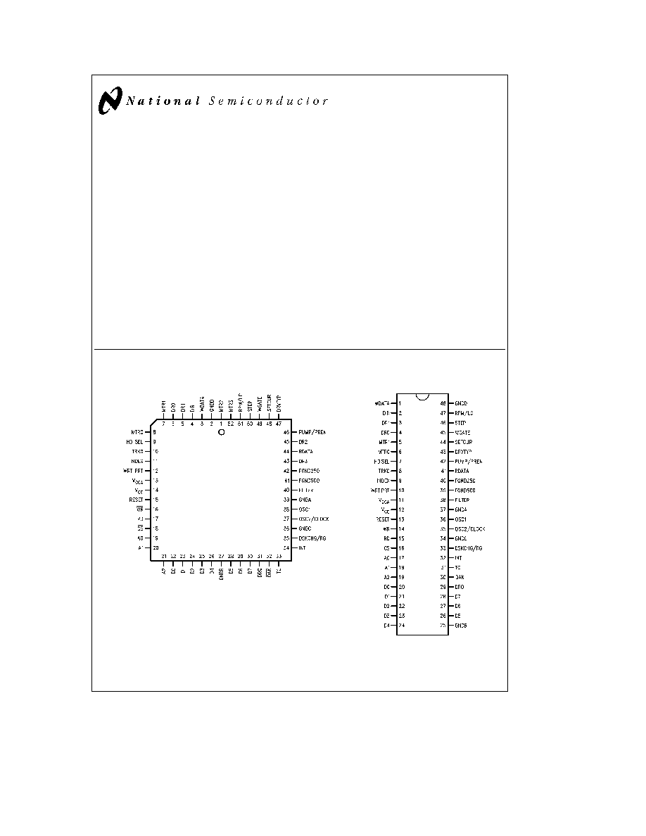
Connection Diagrams
Plastic Leaded Chip Carrier
TL F 9384 1
Top View
Order Number DP8473V
See NS Package Number V52A
Dual-In-Line Package
TL F 9384 2
Top View
Order Number DP8473N
See NS Package Number N48A
TRI-STATE
is a registered trademark of National Semiconductor Corporation
PLUS-2
TM
is a trademark of National Semiconductor Corporation
IBM
PCXT
PCAT
and PS 2
are registered trademarks of International Business Machines Corporation
C1995 National Semiconductor Corporation
RRD-B30M105 Printed in U S A
General Description
(Continued)
the data rate 83 ns 125 ns 208 ns 250 ns for data rates of
1 0M 500k 300k 250 kb s respectively
Specifically to support the PC-AT and PC-XT design the
Floppy Disk Controller PLUS-2 includes address decode for
the A0 A2 address lines the motor drive select register
data rate register for selecting 250 300 500 kb s Disk
Changed status dual speed spindle motor control low write
current and DMA interrupt sharing logic The controller also
supports direct connection to the mP bus via internal 12 mA
buffers The controller also can be connected directly to the
disk drive via internal open drain high drive outputs and
Schmitt inputs
In addition to this logic the DP8473 includes many features
to ease design of higher performance drives and future con-
troller upgrades These include 1 0 Mb s data rate extend-
ed track range to 4096 Implied seeking working Scan Com-
mands motor control timing both standard IBM formats as
well as Sony 3 5
(ISO) formats and other enhancements
This device is available in a 52 pin Plastic Chip Carrier and
in a 48 pin Dual-In-Line package
Table of Contents
General Description
Pin Description
Functional Description
Register Description
Result Phase Register Description
Processor Software Interface
Command Description Table
Command Descriptions
DC and AC Characteristics
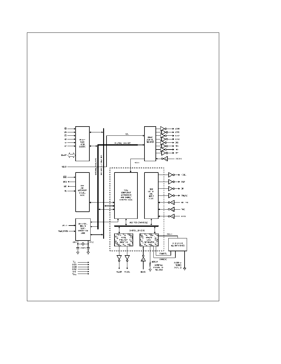
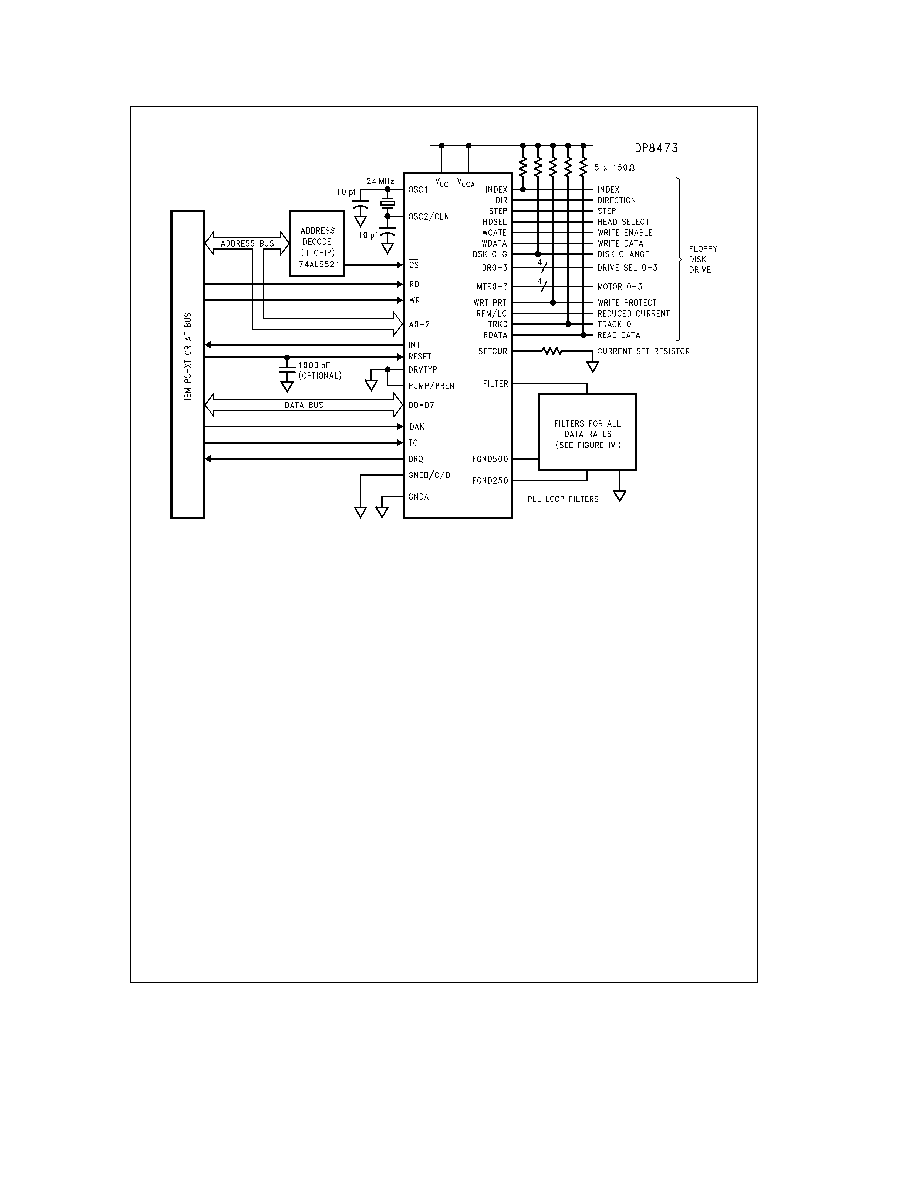
Block Diagram
TL F 9384 3
Note 1
The MTR2 MTR3 DR2 and DR3 are not available on the 48 pin DIP (DP8473N J) versions
Note 2
See
Figure 4 for filter description
Note 3
Total transistor count is 29 700 (approx)
FIGURE 1 DP8473 Functional Block Diagram
2
Pin Descriptions
Symbol
DP8473
DP8473
Function
PCC
DIP
A0 A1 A2
19 21
17 19
Address lines from the microprocessor This determines which registers the
microprocessor is accessing as shown in Table IV in the Register Description Section
Don't care during DMA transfers
CS
18
16
Active low input to enable the RD and WR inputs Not required during DMA transfers
This should be held high during DMA transfers
DAK
32
30
Active low input to acknowledge the DMA request and enable the RD and WR inputs
This signal is enabled when D3 of the Drive Control Register is set
DIR
4
2
This output determines the direction of the head movement (low
e
step in high
e
step
out) When in the write or read modes this output will be high This is a high drive open
drain output
DRQ
31
29
Active high output to signal the DMA controller that a data transfer is needed This signal
is enabled when D3 of the Drive Control Register is set
DRV TYP
47
43
This is an input used by the controller to enable the 300 kb s mode This enables the use
of floppy drives with either dual or single speed spindle motors For dual speed spindle
motors this pin is tied low When low and 300 kb s data rate is selected in the data rate
register the PLL actually uses 250 kb s This pin is tied high for single speed spindle
motor drives (standard AT drive) When this pin is high and 300 kb s is selected 300 kb s
is used (See also RPM LC pin)
DR0
6
4
This is an active low drive select line for drive 0 that is controlled by the Drive Control
register bits D0 D1 The Drive Select bit is ANDed with the Motor Enable of the same
number This is a high drive open drain output
DR1
5
3
This is an active low drive select similar to DR0 line except for drive 1
DR2
45
This is the same as DR0 except for drive 2
DR3
43
This is the same as DR0 except for drive 3
DSKCHG RG
35
33
This latched Schmitt input signal is inverted and routed to D7 of the data bus and is read
when address xx7H is enabled DSKCHG is a disk drive output that indicates when the
drive door has been opened When the RG bit in the Mode Command is set this pin
functions as a Read Gate signal that when low forces the data separator to lock to the
crystal and when high it locks to data for diagnostic purposes
D0 D4
22-26
20 24
Bi-directional data lines to the microprocessor These are the lower 5 bits and have
buffered 12 mA outputs
D5 D7
28 30
26 28
Bi-directional data lines to the microprocessor These upper 3 bits have buffered 12 mA
outputs
FGND250
42
40
This pin connects the PLL filter for 250k(MFM) 125k(FM) b s or 300k(MFM) 150k(FM)
b s to ground This is a low impedance open drain output
FGND500
41
39
This pin connects the PLL filter for 500k(MFM) 250k(FM) b s to ground This is a low
impedance open drain output
FILTER
40
38
This pin is the output of the charge pump and the input to the VCO One or more filters
are attached between this pin and the GNDA FGND250 and FGND500 pins
GNDA
39
37
This pin is the analog ground for the data separator including all primary and secondary
PLLs and delay lines
GNDB
27
25
This pin is the digital ground for the 12 mA microprocessor interface buffers This
includes D0 D7 INT and DRQ
GNDC
36
34
This pin is the digital ground for the controller's digital logic including all internal registers
micro-engine etc
GNDD
2
48
This pin is the digital ground for the disk interface output drivers
HD SEL
9
7
This output determines which disk drive head is active Low
e
Head 1 Open (high)
e
Head 0 This is a high drive open drain output
INDEX
11
9
This active low Schmitt input signals the beginning of a track
INT
34
32
Active high output to signal that an operation requires the attention of the
microprocessor The action required depends on the current function of the controller
This signal is enabled when D3 of the Drive Control Register is set
3
Pin Descriptions
(Continued)
Symbol
DP8473
DP8473
Function
PCC
DIP
MTR0
8
6
This is an active low motor enable line for drive 0 which is controlled by the Drive Control
register This is a high drive open drain output
MTR1
7
5
This is an active low motor enable line for drive 1 Similar to MTR0
MTR2
1
This is an active low motor enable line for drive 2 Similar to MTR0
MTR3
52
This is an active low motor enable line for drive 3 Similar to MTR0
OSC1
38
36
One side of an external 24 MHz crystal is attached here This pin is tied low if an external
clock is used
OSC2 CLOCK
37
35
One side of the external 24 MHz crystal is attached here If a crystal is not used a TTL or
CMOS compatible clock is connected to this pin
PUMP PREN
46
42
When the PU bit is set in Mode Command this pin is an output that indicates when the
charge pump is making a correction Otherwise this pin is an input that sets the precomp
mode as shown in Table VI If pin is configured as PUMP PREN is assumed high
RD
17
15
Active low input to signal a read from the controller to the microprocessor
RDATA
44
41
The active low raw data read from the disk is connected here This is a Schmitt input
RESET
15
13
Active high input that resets the controller to the idle state and resets all the output lines
to the disk drive to their disabled state The Drive Control register is reset to 00 The Data
Rate register is set to 250 kb s The Specify command registers are not affected The
Mode Command registers are set to the default values Reset should be held active
during power up To prevent glitches activating the reset sequence a small capacitor
(1000 pF) should be attached to this pin
RPM LC
51
47
This high drive open drain output pin has two functions based on the selection of the
DRVTYP pin
1 When using a dual speed spindle motor floppy drive (DRVTYP pin low) this output is
used to select the spindle motor speed either 300 RPM or 360 RPM In this mode this
output goes low when 250 300 kb data rate is chosen in the data rate register and high
when 500 kb s is chosen
2 When using a single speed spindle motor floppy drive (DRVTYP pin high) this pin
indicates when to reduce the write current to the drive This output is high for high density
media (when 500 kb s is chosen)
SETCUR
48
44
An external resistor connected from this pin to analog ground programs the amount of
charge pump current that drives the external filters The PLL Filter Design section shows
how to determine the values
STEP
50
46
This active low open drain high drive output will produce a pulse at a software
programmable rate to move the head during a seek operation
TC
33
31
Active high input to indicate the termination of a DMA transfer This signal is enabled
when the DMA Acknowledge pin is active
TRK0
10
8
This active low Schmitt input tells the controller that the head is at track zero of the
selected disk drive
WDATA
3
1
This is the active low open drain write precompensated serial data to be written onto the
selected disk drive This is a high drive open drain output
WGATE
49
45
This active low open drain high drive output enables the write circuitry of the selected
disk drive This output has been designed to prevent glitches during power up and power
down This prevents writing to the disk when power is cycled
WR
16
14
Active low input to signal a write from the microprocessor to the controller
WRT PRT
12
10
This active low Schmitt input indicates that the disk is write protected Any command that
writes to that disk drive is inhibited when a disk is write protected
V
CC
14
12
This pin is the 5V supply for the digital circuitry
V
CCA
13
11
This pin is the 5V supply for the analog data separator circuitry
4
Typical Application
TL F 9384 4
Recommended Plastic Chip Carrier Socket
AMP P N 821551-1 or equivalent
FIGURE 2 DP8473 Typical Application
Functional Description
This section describes the basic architectural features of
the DP8473 and many of the enhancements provided Re-
fer to
Figure 1
765A COMPATIBLE MICRO-ENGINE
The core of the DP8473 is a mPD765A compatible micro-
coded engine This engine consists of a sequencer pro-
gram ROM and disk misc registers This core is clocked by
either a 4 MHz 4 8 MHz or 8 MHz clock selected in the Data
Rate Register Upon this core is added all the glue logic
used to implement a PC-XT or AT or PS 2 floppy controller
as well as the data separator and write precompensation
logic
The controller consists of a microcoded engine that controls
the entire operation of the chip including coordination of
data transfer with the CPU controlling the drive controls
and actually performing the algorithms associated with
reading and writing data to from the disk This includes the
read algorithm for the data separator
Like the mPD765A this controller takes commands and re-
turns data and status through the Data Register in a byte
serial fashion Handshake for command status I O is pro-
vided via the Main Status Register All of the mPD765A
commands are supported as are many other enhanced
commands
DATA SEPARATOR
The internal data separator consists of an analog PLL and
its associated circuitry The PLL synchronizes the raw data
signal read from the disk drive The synchronized signal is
used to separate the encoded clock and data pulses The
data pulses are de-serialized into bytes and then sent to the
m
P by the controller
The main PLL consists of four main components a phase
comparator a filter a voltage controlled oscillator (VCO)
and a programmable divider The phase comparator detects
the difference between the phase of the divider's output and
the phase of the raw data being read from the disk This
phase difference is converted to a current which either
charges or discharges one of the three external filters The
resulting voltage on the filter changes the frequency of the
VCO and the divider output to reduce the phase difference
between the input data and the divider's output The PLL is
``locked'' when the frequency of the divider is exactly the
same as the average frequency of the data read from the
disk A block diagram of the data separator is shown in
Fig-
ure 3
5