
DS14185
EIA/TIA-232
3 Driver x 5 Receiver
General Description
The DS14185 is a three driver, five receiver device which
conforms to the EIA/TIA-232-E standard.
The flow-through pinout facilitates simple non-crossover
board layout. The DS14185 provides a one-chip solution for
the common 9-pin serial RS-232 interface between data ter-
minal and data communications equipment.
Features
n
Replaces one 1488 and two 1489s
n
Conforms to EIA/TIA-232-E
n
3 drivers and 5 receivers
n
Flow through pinout
n
Failsafe receiver outputs
n
20-pin SOIC package
n
LapLink
Æ
compatible -200 kbps data rate
Connection Diagram
Functional Diagram
LapLink
Æ
is a registered trademark of Travelling Software.
SOIC
DS011938-1
Order Number DS14185WM
See NS Package M20B
DS011938-2
April 1999
DS14185
EIA/TIA-232
3
Drive
r
x
5
Receiver
© 1999 National Semiconductor Corporation
DS011938
www.national.com

Absolute Maximum Ratings
(Note 1)
If Military/Aerospace specified devices are required,
please contact the National Semiconductor Sales Office/
Distributors for availability and specifications.
Supply Voltage (V
CC
)
+7V
Supply Voltage (V
+
)
+15V
Supply Voltage (V
-
)
-15V
Driver Input Voltage
0V to V
CC
Driver Output Voltage (Power
Off)
±
15V
Receiver Input Voltage
±
25V
Receiver Output Voltage (R
OUT
)
0V to V
CC
Maximum Package Power Dissipation
@
+25∞C
M Package
1488 mW
Derate M Package
11.9 mW/∞C above +25∞C
Storage Temperature Range
-65∞C to +150∞C
Lead Temperature Range
(Soldering, 4 seconds)
+260∞C
ESD Ratings (HBM, 1.5 k
, 100
pF)
1.5 kV
Recommended Operating
Conditions
Min
Typ
Max
Units
Supply Voltage (V
CC
)
+4.75
+5.0
+5.25
V
Supply Voltage (V
+
)
+9.0
+12.0
+13.2
V
Supply Voltage (V
-
)
-13.2
-12.0
-9.0
V
Operating Free Air
Temperature (T
A
)
0
25
70
∞C
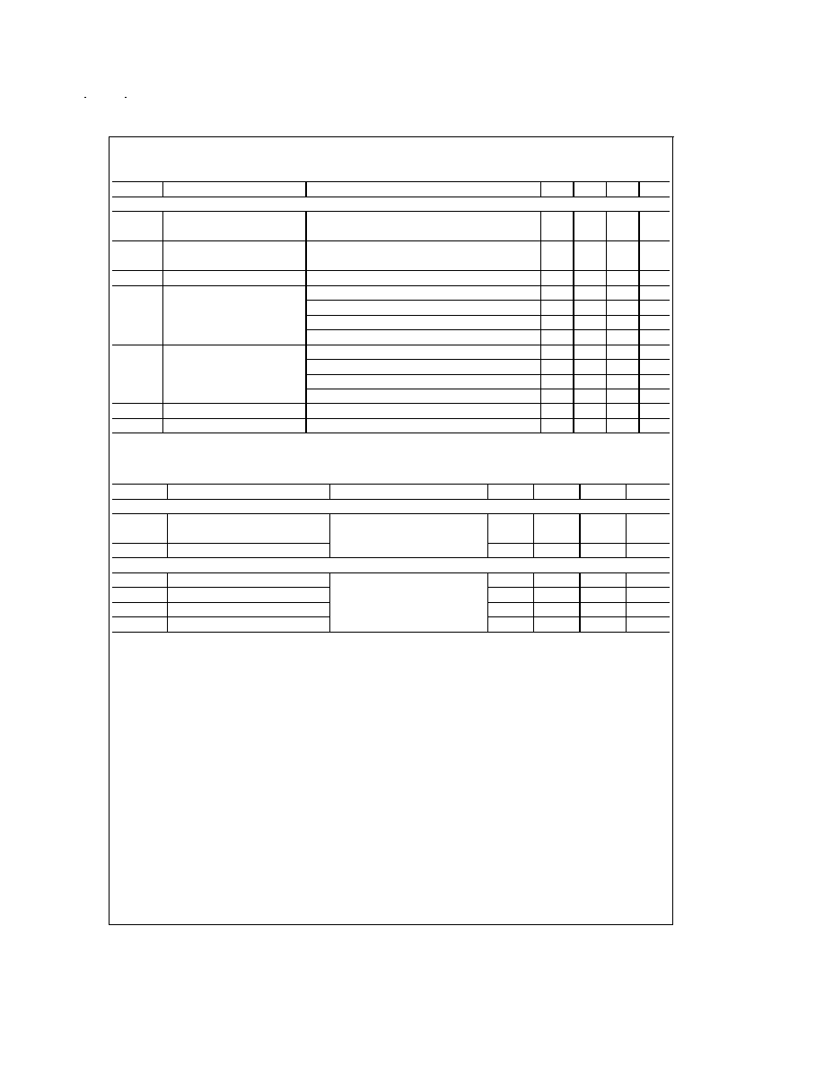
Electrical Characteristics
(Note 2)
Over recommended supply voltage and operating temperature ranges, unless otherwise specified.
Symbol
Parameter
Conditions
Min
Typ
Max
Units
DEVICE CHARACTERISTICS
I
CC
V
CC
Supply Current
No Load, All Inputs at +5V
21.0
30
mA
I
+
V
+
Supply Current
(Note 2)
No Load, All Driver
Inputs at 0.8V or +2V
All Receiver Inputs
at 0.8V or 2.4V.
V
+
= 9V, V
-
= -9V
8.7
15
mA
V
+
= 13.2V, V
-
= -13.2V
13
22
mA
I
-
V
-
Supply Current
(Note 2)
V
+
= 9V, V
-
= -9V
-12.5
-22
mA
V
+
= 13.2V, V
-
= -13.2V
-16.5
-28
mA
DRIVER CHARACTERISTICS
V
IH
High Level Input Voltage
2.0
V
V
IL
Low Level Input Voltage
0.8
V
I
IH
High Level Input Current
V
IN
= 5V
10
µA
(Note 2)
I
IL
Low Level Input Current
V
IN
= 0V
-1.24
-1.5
mA
(Note 2)
V
OH
High Level Output Voltage
R
L
= 3 k
, V
IN
= 0.8V,
6
7
V
(Note 2)
V
+
= 9V, V
-
= -9V
R
L
= 3 k
, V
IN
= 0.8V,
8.5
9
V
V
+
= +12V, V
-
= -12V
R
L
= 7 k
, V
IN
= 0.8V,
10
11.5
V
V
+
= +13.2V, V
-
= -13.2V
V
OL
Low Level Output Voltage
R
L
= 3 k
, V
IN
= 2V,
-7
-6
V
(Note 2)
V
+
= 9V, V
-
= -9V
R
L
= 3 k
, V
IN
= 2V,
-8
-7.5
V
V
+
= +12V, V
-
= -12V
R
L
= 7 k
, V
IN
= 0.8V,
-11
-10
V
V
+
= +13.2V, V
-
= -13.2V
I
OS
+
Output High Short
V
O
= 0V, V
IN
= 0.8V
-6
-13
-18
mA
Circuit Current (Note 2)
I
OS
-
Output Low Short
V
O
= 0V, V
IN
= 2.0V
6
13
18
mA
Circuit Current (Note 2)
R
O
Output Resistance
-2V
V
O
+2V,
300
V
+
= V
-
= V
CC
= 0V
-2V
V
O
+2V,
300
V
+
= V
-
= V
CC
= Open Ckt
www.national.com
2
Electrical Characteristics
(Note 2) (Continued)
Over recommended supply voltage and operating temperature ranges, unless otherwise specified.
Symbol
Parameter
Conditions
Min
Typ
Max
Units
RECEIVER CHARACTERISTICS
V
TH
Input High Threshold
V
O
0.4V, I
O
= 3.2 mA
1.85
2.4
V
(Recognized as a High Signal)
V
TL
Input Low Threshold
V
O
2.5V, I
O
= -0.5 mA
0.7
1.0
V
(Recognized as a Low Signal)
R
IN
Input Resistance
V
IN
=
±
3V to
±
15V
3.0
4.1
7.0
k
I
IN
Input Current (Note 2)
V
IN
= +15V
2.1
4.1
5.0
mA
V
IN
= +3V
0.43
0.7
1
mA
V
IN
= -15V
-5.0
-4.1
-2.1
mA
V
IN
= -3V
-1
-0.65
-0.43
mA
V
OH
High Level Output Voltage
I
OH
= -0.5 mA, V
IN
= -3V
2.6
4
V
(Note 7)
I
OH
= -10 µA, V
IN
= -3V
4.0
4.9
V
I
OH
= -0.5 mA, V
IN
= Open Circuit
2.6
4
V
I
OH
= -10 µA, V
IN
= Open Circuit
4.0
4.9
V
V
OL
Low Level Output Voltage
I
OL
= 3.2 mA, V
IN
= +3V
0.2
0.4
V
I
OSR
Short Circuit Current (Note 2)
V
O
= 0V, V
IN
= 0V
-4
-2.7
-1.7
mA
Switching Characteristics
(Note 2)
T
A
= 25∞C
Symbol
Parameter
Conditions
Min
Typ
Max
Units
DRIVER CHARACTERISTICS
t
PHL
Propagation Delay High to Low
R
L
= 3 k
, C
L
= 50 pF
(
Figures 1, 2)
60
350
ns
t
PLH
Propagation Delay Low to High
240
350
ns
t
r
, t
f
Output Slew Rate (Note 8)
50
ns
RECEIVER CHARACTERISTICS
t
PHL
Propagation Delay High to Low
R
L
= 1.5 k
, C
L
= 15 pF
(includes fixture plus probe),
(
Figures 3, 4)
150
350
ns
t
PLH
Propagation Delay Low to High
240
350
ns
t
r
Rise Time
87
175
ns
t
f
Fall Time
40
100
ns
Note 1: Absolute Maximum Ratings are those values beyond which the safety of the device cannot be guaranteed. They are not meant to imply that the devices
should be operated at these limits. The table of Electrical Characteristics specifies conditions of device operation.
Note 2: Current into device pins is defined as positive. Current out of device pins is defined as negative. All voltages are referenced to ground unless otherwise speci-
fied. For current, minimum and maximum values are specified as an absolute value and the sign is used to indicate direction. For voltage logic levels, the more posi-
tive value is designated as maximum. For example, if -6V is a maximum, the typical value (-6.8V) is more negative.
Note 3: All typicals are given for: V
CC
= +5.0V, V
+
= +12.0V, V
-
= -12V, T
A
= +25∞C.
Note 4: Only one driver output shorted at a time.
Note 5: Generator characteristics for driver input: f = 64 kHz (128 kbits/sec), t
r
= t
f
<
10 ns, V
IH
= 3V, V
IL
= 0V, duty cycle = 50%.
Note 6: Generator characteristics for receiver input: f = 64 kHz (128 kbits/sec), t
r
= t
f
= 200 ns, V
IH
= 3V, V
IL
= -3V, duty cycle = 50%.
Note 7: If receiver inputs are unconnected, receiver output is a logic high.
Note 8: Refer to typical curves. Driver output slew rate is measured from the +3.0V to the -3.0V level on the output waveform. Inputs not under test are connected
to V
CC
or GND. Slew rate is determined by load capacitance. To comply with a 30 V/µs maximum slew rate, a minimum load capacitance of 390 pF is recommended.
www.national.com
3

Parameter Measurement Information
Pin Descriptions
Pin #
Name
Description
13, 15, 16
D
IN
Driver Input Pins
5, 6, 8
D
OUT
Driver Output Pins, RS-232 Levels
2, 3, 4, 7, 9
R
IN
Receiver Input Pins, RS-232 Levels
12, 14, 17, 18, 19
R
OUT
Receiver Output Pins
11
GND
Ground
1
V
+
Positive Power Supply Pin (+9.0
V
+
+13.2)
DS011938-3
FIGURE 1. Driver Propagation Delay and Transition Time Test Circuit (Note 5)
DS011938-4
FIGURE 2. Driver Propagation Delay and Transition Time Waveforms Slew Rate (SR) = 6V/(t
r
or t
f
)
DS011938-5
FIGURE 3. Receiver Propagation Delay and Transition Time Test Circuit (Note 6)
DS011938-6
FIGURE 4. Receiver Propagation Delay and
Transition Time Waveform
www.national.com
4
Pin Descriptions
(Continued)
Pin #
Name
Description
10
V
-
Negative Power Supply Pin (-9.0
V
-
-13.2)
20
V
CC
Positive Power Supply Pin (+5V
±
5%)
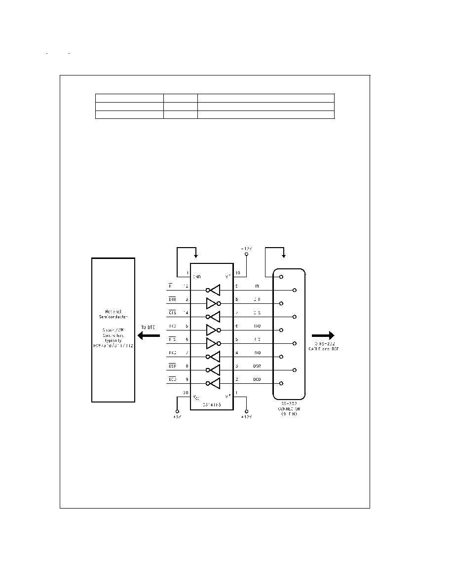
Applications Information
In a typical Data Terminal Equipment (DTE) to Data
Circuit-Terminating Equipment (DCE) 9-pin de-facto inter-
face implementation, 2 data lines and 6 control lines are re-
quired. The data lines are TXD and RXD. The control lines
are RTS, DTR, DSR, DCD, CTS, and RI.
The DS14185 is a 3 x 5 Driver/Receiver and offers a single
chip solutuion for this DTE interface. As shown in
Figure 5,
this interface allows for direct flow-thru interconnect. For a
more conservative design, the user may wish to insert
ground traces between the signal lines to minimize cross
talk.
LapLink COMPATIBILITY
The DS14185 can easily provide 128 kbps data rate under
maximum driver load conditions of C
L
= 2500 pF and R
L
= 3
k
, while power supplies are:
V
CC
= 4.75V, V
+
= 10.8V, V
-
= -10.8V
MOUSE DRIVING
A typical mouse can be powered from the drivers. Two driver
outputs connected in parallel and set to V
OH
can be used to
supply power to the V
+
pin of the mouse. The third driver out-
put is set to V
OL
to sink the current from the V
-
terminal. Re-
fer to typical curves of V
OUT
/I
OUT
.Typical mouse specifica-
tions are:
10 mA at +6V
5 mA at -6V
DS011938-7
FIGURE 5. Typical DTE Application
www.national.com
5