 | –≠–ª–µ–∫—Ç—Ä–æ–Ω–Ω—ã–π –∫–æ–º–ø–æ–Ω–µ–Ω—Ç: DS1488N | –°–∫–∞—á–∞—Ç—å:  PDF PDF  ZIP ZIP |

DS1488
Quad Line Driver
General Description
The DS1488 is a quad line driver which converts standard
TTL input logic levels through one stage of inversion to out-
put levels which meet EIA Standard RS-232D and CCITT
Recommendation V.24.
Features
n
Current limited output:
±
10 mA typ
n
Power-off source impedance:
300
min
n
Simple slew rate control with external capacitor
n
Flexible operating supply range
n
Inputs are TTL/LS compatible
Schematic and Connection Diagrams
1/4 Circuit
DS005776-1
Dual-In-Line Package
DS005776-2
Top View
Order Number DS1488M or DS1488N
See NS Package Number M14A or N14A
July 1999
DS1488
Quad
Line
Driver
© 1999 National Semiconductor Corporation
DS005776
www.national.com

Absolute Maximum Ratings
(Note 2)
If Military/Aerospace specified devices are required,
please contact the National Semiconductor Sales Office/
Distributors for availability and specifications.
Supply Voltage
V
+
+15V
V
-
-15V
Input Voltage (V
IN
)
-15V
V
IN
7.0V
Output Voltage
±
15V
Operating Temperature Range
0∞C to +75∞C
Storage Temperature Range
-65∞C to +150∞C
Maximum Power Dissipation (Note 1) at 25∞C
Molded DIP Package
1280 mW
SO Package
974 mW
Lead Temperature (Soldering, 4
sec.)
260∞C
Note 1: Derate molded DIP package 10.2 mW/∞C above 25∞C; derate SO
package 7.8 mW/∞C above 25∞C.
Electrical Characteristics
(Notes 3, 4)
V
CC
+ = 9V, V
CC
- = -9V unless otherwise specified
Symbol
Parameter
Conditions
Min
Typ
Max
Units
I
IL
Logical "0" Input Current
V
IN
= 0V
-0.8
-1.3
mA
I
IH
Logical "1" Input Current
V
IN
= +5.0V
0.005
10.0
µA
V
OH
High Level Output Voltage
R
L
= 3.0 k
,
V
+
= 9.0V, V
-
= -9.0V
6.0
7.1
V
V
IN
= 0.8V
V
+
= 13.2V, V
-
= -13.2V
9.0
10.7
V
V
OL
Low Level Output Voltage
R
L
= 3.0 k
,
V
+
= 9.0V, V
-
= -9.0V
-6.0
7.0
V
V
IN
= 1.9V
V
+
= 13.2V, V
-
= -13.2V
-9.0
-10.6
V
I
OS
+
High Level Output
V
OUT
= 0V, V
IN
= 0.8V
-6.0
-10.0
-12.0
mA
Short-Circuit Current
I
OS
-
Low Level Output
V
OUT
= 0V, V
IN
= 1.9V
6.0
10.0
12.0
mA
Short-Circuit Current
R
OUT
Output Resistance
V
+
= V
-
= 0V, V
OUT
=
±
2V
300
I
CC
+
Positive Supply Current
V
IN
= 1.9V
V
+
= 9.0V, V
-
= -9.0V
11.6
20.0
mA
(Output Open)
V
+
= 12V, V
-
= -12V
15.7
25.0
mA
V
+
= 15V, V
-
= -15V
19.4
34.0
mA
V
IN
= 0.8V
V
+
= 9.0V, V
-
= -9.0V
3.4
6.0
mA
V
+
= 12V, V
-
= -12V
4.1
7.0
mA
V
+
= 15V, V
-
= -15V
9.1
12.0
mA
I
CC
-
Negative Supply Current
V
IN
= 1.9V
V
+
= 9.0V, V
-
= -9.0V
-10.8
-17.0
mA
(Output Open)
V
+
= 12V, V
-
= -12V
-14.6
-23.0
mA
V
+
= 15V, V
-
= -15V
-18.3
-34.0
mA
V
IN
= 0.8V
V
+
= 9.0V, V
-
= -9.0V
-0.001
-0.100
mA
V
+
= 12V, V
-
= -12V
-0.001
-0.100
mA
V
+
= 15V, V
-
= -15V
-0.01
-2.5
mA
P
d
Power Dissipation
V
+
= 9.0V, V
-
= -9.0V
252
333
mW
V
+
= 12V, V
-
= -12V
444
576
mW
Switching Characteristics
(V
CC
= 9V, V
EE
= -9V, T
A
= 25∞C)
Symbol
Parameter
Conditions
Min
Typ
Max
Units
t
pd1
Propagation Delay to a Logical "1"
R
L
= 3.0 k
, C
L
= 15 pF, T
A
= 25∞C
187
350
ns
t
pd0
Propagation Delay to a Logical "0"
R
L
= 3.0 k
, C
L
= 15 pF, T
A
= 25∞C
45
175
ns
t
r
Rise Time
R
L
= 3.0 k
, C
L
= 15 pF, T
A
= 25∞C
63
100
ns
t
f
Fall Time
R
L
= 3.0 k
, C
L
= 15 pF, T
A
= 25∞C
33
75
ns
Note 2: "Absolute Maximum Ratings" are those values beyond which the safety of the device cannot be guaranteed. Except for "Operating Temperature Range" they
are not meant to imply that the devices should be operated at these limits. The table of "Electrical Characteristics" provides conditions for actual device operation.
Note 3: Unless otherwise specified min/max limits apply across the 0∞C to +75∞C temperature range for the DS1488.
Note 4: All currents into device pins shown as positive, out of device pins as negative, all voltages referenced to ground unless otherwise noted. All values shown
as max or min on absolute value basis.
www.national.com
2
Applications
By connecting a capacitor to each driver output the slew
rate can be controlled utilizing the output current limiting
characteristics of the DS1488. For a set slew rate the ap-
propriate capacitor value may be calculated using the fol-
lowing relationship
C = I
SC
(
T/
V)
where C is the required capacitor, I
SC
is the short circuit
current value, and
V/
T is the slew rate.
RS-232C specifies that the output slew rate must not ex-
ceed 30V per microsecond. Using the worst case output
short circuit current of 12 mA in the above equation, calcu-
lations result in a required capacitor of 400 pF connected
to each output.
See Typical Performance Characteristics.
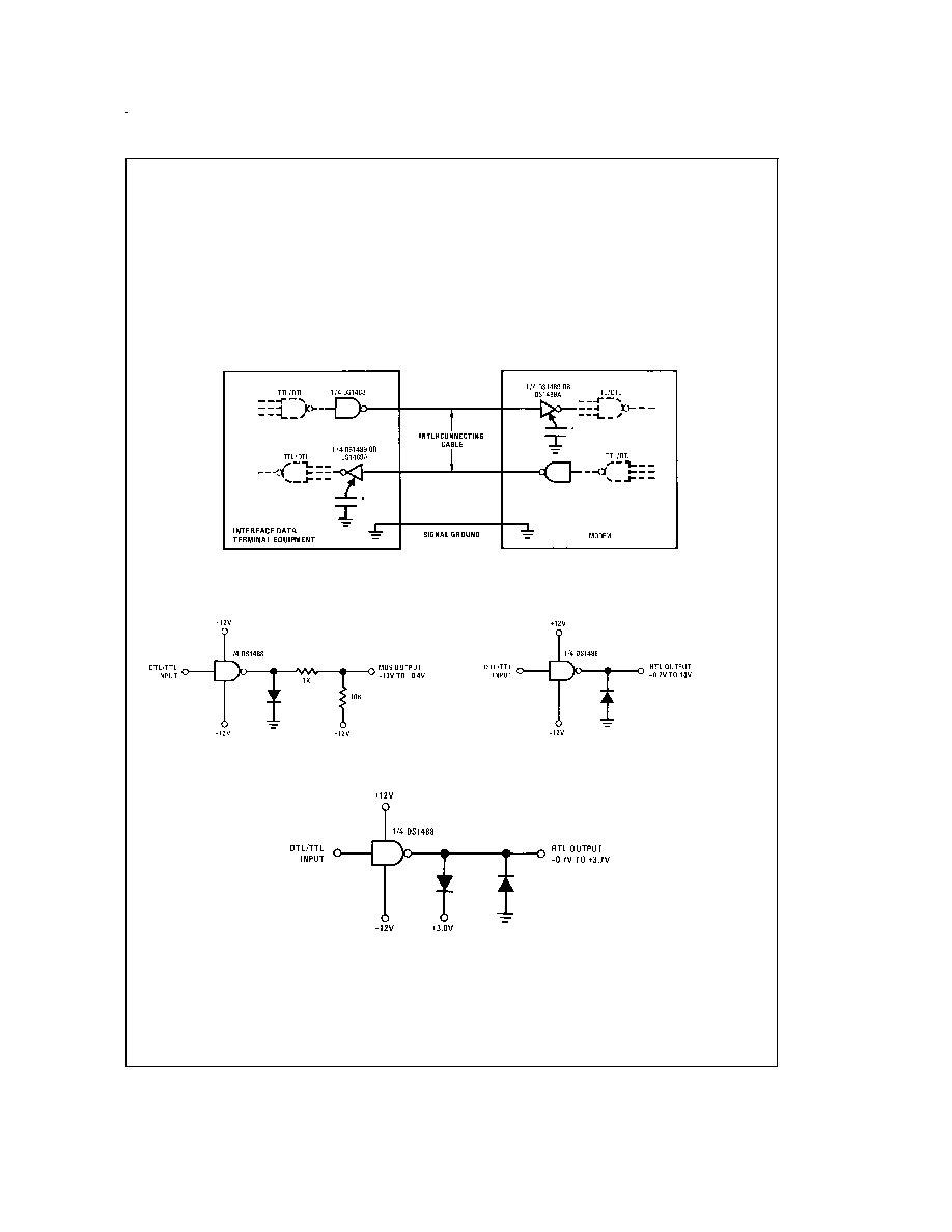
Typical Applications
RS-232C Data Transmission
DS005776-3
Note 5: Optional for noise filtering
DTL/TTL-to-MOS Translator
DS005776-4
DTL/TTL-to-HTL Translator
DS005776-5
DTL/TTL-to-RTL Translator
DS005776-6
www.national.com
3
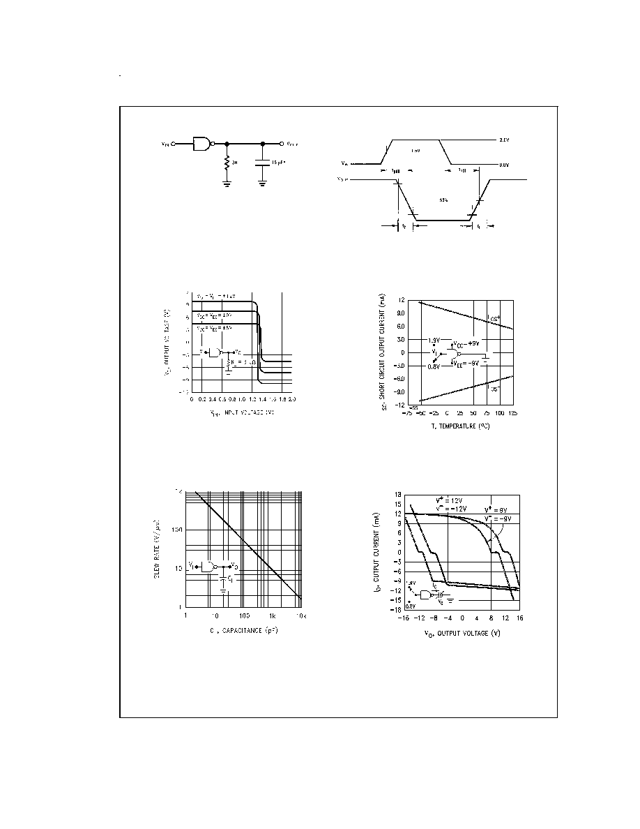
AC Load Circuit and Switching Time Waveforms
Typical Performance Characteristics
T
A
=+25∞C unless otherwise noted
DS005776-7
*
C
L
includes probe and jig capacitance.
DS005776-8
t
r
and t
f
are measured between 10%
and 90% of the output waveform.
DS005776-9
FIGURE 1. Transfer Characteristics
vs Power Supply Voltage
DS005776-10
FIGURE 2. Short-Circuit Output
Current vs Temperature
DS005776-11
FIGURE 3. Output Slew Rate vs
Load Capacitance
DS005776-12
FIGURE 4. Output Voltage and
Current-Limiting Characteristics
www.national.com
4

Physical Dimensions
inches (millimeters) unless otherwise noted
SO Package (M)
Order Number DS1488M
NS Package Number M14A
Molded Dual-In-Line Package (N)
Order Number DS1488N
NS Package Number N14A
www.national.com
5