
DS14C232
Low Power +5V Powered TIA/EIA-232 Dual
Driver/Receiver
General Description
The DS14C232 is a low power dual driver/receiver featuring
an onboard DC to DC converter, eliminating the need for
±
12V power supplies. The device only requires a +5V power
supply. I
CC
is specified at 3.0 mA maximum, making the de-
vice ideal for battery and power conscious applications. The
drivers' slew rate is set internally and the receivers feature
internal noise filtering, eliminating the need for external slew
rate and filter capacitors. The device is designed to interface
data terminal equipment (DTE) with data circuit-terminating
equipment (DCE). The driver inputs and receiver outputs are
TTL and CMOS compatible. DS14C232C driver outputs and
receiver inputs meet TIA/EIA-232-E (RS-232) and CCITT
V.28 standards.
Features
n
Pin compatible with industry standard MAX232, LT1081,
ICL232 and TSC232
n
Single +5V power supply
n
Low power -- I
CC
3.0 mA maximum
n
DS14C232C meets TIA/EIA-232-E (RS-232) and CCITT
V.28 standards
n
CMOS technology
n
Receiver Noise Filter
n
Package efficiency -- 2 drivers and 2 receivers
n
Available in Plastic DIP, Narrow and Wide SOIC
packages
n
TIA/EIA-232 compatible extended temperature range
option:
DS14C232T
-40∞C to +85∞C
DS14C232E/J:
-55∞C to +125∞C
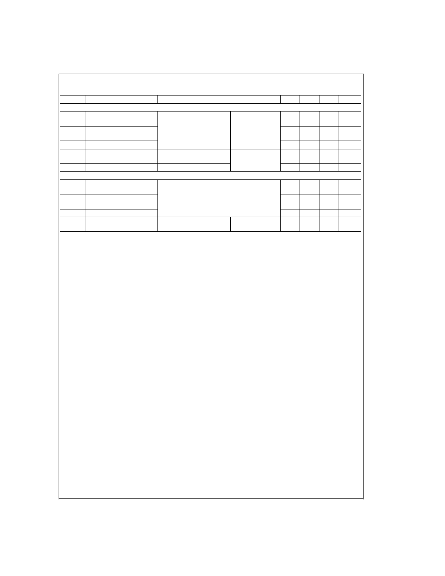
Connection Diagram
Functional Diagram
DS010744-1
Order Number DS14C232CN, DS14C232CM, or
DS14C232TM
See NS Package Number N16E, or M16A
DS010744-2
October 1999
DS14C232
Low
Power
+5V
Powered
TIA/EIA-232
Dual
Driver/Receiver
© 1999 National Semiconductor Corporation
DS010744
www.national.com

Absolute Maximum Ratings
(Note 1)
Specifications for the 883 version of this product are
listed separately on the following pages.
Supply Voltage, V
CC
-0.3V to 6V
V
+
Pin
(V
CC
- 0.3)V to +14V
V
-
Pin
+0.3V to -14V
Driver Input Voltage
-0.3V to (V
CC
+ 0.3V)
Driver Output Voltage
(V
+
+ 0.3V) to (V
-
-
0.3V)
Receiver Input Voltage
±
25V
Receiver Output Voltage
-0.3V to (V
CC
+ 0.3V)
Junction Temperature
+150∞C
Maximum Package Power Dissipation
@
25∞C (Note 6)
N Package
1698 mW
M Package
1156 mW
Short Circuit Duration,
D
OUT
Continuous
Storage Temp. Range
-65∞C to +150∞C
Lead Temp. (Soldering, 4
sec.)
+260∞C
ESD Rating
(HBM, 1.5 k
, 100 pF)
2.5 kV
Recommended Operating
Conditions
Min
Max
Units
Supply Voltage, V
CC
4.5
5.5
V
Operating Free Air Temp. (T
A
)
DS14C232C
0
+70
∞C
DS14C232T
-40
+85
∞C
Electrical Characteristics
(Note 2)
Over recommended operating conditions, unless otherwise specified
Symbol
Parameter
Conditions
Min
Typ
Max
Units
DC TO DC CONVERTER CHARACTERISTICS
V
+
Positive Power Supply
R
L
= 3 k
, C1≠C4 = 1.0 µF, D
IN
= 0.8V
9.0
V
V
-
Negative Power Supply
R
L
= 3 k
, C1≠C4 = 1.0 µF, D
IN
= 2.0V
-8.5
V
I
CC
Supply (V
CC
) Current
No Load
1.0
3.0
mA
DRIVER CHARACTERISTICS
V
IH
High Level Input Voltage
2
V
CC
V
V
IL
Low Level Input Voltage
GND
0.8
V
I
IH
High Level Input Current
V
IN
2.0V
-10
+10
µA
I
IL
Low Level Input Current
V
IN
0.8V
-10
+10
µA
V
OH
High Level Output Voltage
R
L
= 3 k
5.0
8.0
V
V
OL
Low Level Output Voltage
R
L
= 3 k
-7.0
-5.0
V
I
OS+
Output High Short Circuit
Current
V
O
= 0V, V
IN
= 0.8V
(Note 3)
-30
-15
-5.0
mA
I
OS-
Output Low Short Circuit
Current
V
O
= 0V, V
IN
= 2V
5.0
11
30
mA
R
O
Output Resistance
-2V
V
O
+2V,
300
V
CC
= 0V = GND
RECEIVER CHARACTERISTICS
V
TH
Input High Threshold
Voltage
V
CC
= 5.0V
1.9
2.4
V
V
CC
= 5.0V
±
10%
1.9
2.6
V
V
TL
Input Low Threshold
Voltage
0.8
1.5
V
V
HY
Hysteresis
0.2
0.4
1.0
V
R
IN
Input Resistance
-15V
V
IN
+15V
3.0
4.7
7.0
k
I
IN
Input Current
V
IN
= +15V
+2.14
+3.75
+5.0
mA
V
IN
= +3V
+0.43
+0.64
+1.0
mA
V
IN
= -3V
-1.0
-0.64
-0.43
mA
V
IN
= -15V
-5.0
-3.75
-2.14
mA
V
OH
High Level Output Voltage
V
IN
= -3V, I
O
= -3.2 mA
3.5
4.5
V
V
IN
= -3V, I
O
= -20 µA
4.0
4.9
V
V
OL
Low Level Output Voltage
V
IN
= +3V, I
O
= +3.2 mA
0.15
0.4
V
DS14C232
www.national.com
2
Switching Characteristics
Over recommended operating conditions, unless otherwise specified.
Symbol
Parameter
Conditions
Min
Typ
Max
Units
DRIVER CHARACTERISTICS
t
PLH
Propagation Delay Low to
High
R
L
= 3 k
C
L
= 50 pF
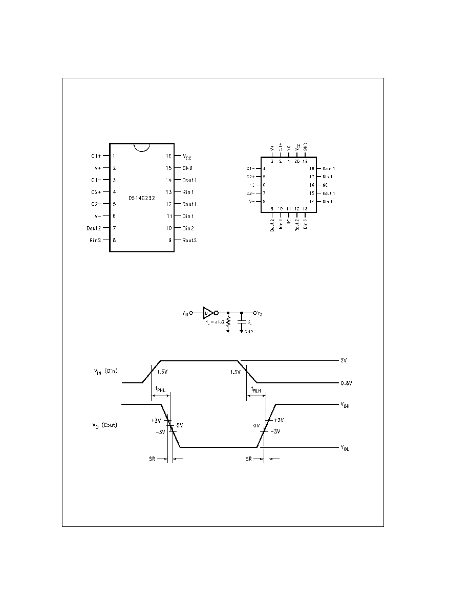
Figure 1
and
Figure 2
1.0
4.0
µs
t
PHL
Propagation Delay High to
Low
1.0
4.0
µs
t
SK
Skew |t
PLH
- t
PHL
|
0.1
1.0
µs
SR1
Output Slew Rate
R
L
= 3 k
to 7 k
, C
L
=
50 pF
(Note 7)
4.0
30
V/µs
SR2
Output Slew Rate
R
L
= 3 k
, C
L
= 2500 pF
4.5
V/µs
RECEIVER CHARACTERISTICS
t
PLH
Propagation Delay Low to
High
Input Pulse Width
>
10 µs
2.9
6.5
µs
t
PHL
Propagation Delay High to
Low
C
L
= 50 pF
2.5
6.5
µs
t
SK
Skew |t
PLH
- t
PHL
|
(
Figures 3, 4)
0.4
2.0
µs
t
nw
Noise Pulse Width
Rejected
(
Figures 3, 4)
0.7
0.5
µs
Note 1: "Absolute Maximum Ratings" are those values beyond which the safety of the device cannot be guaranteed. They are not meant to imply that the devices
should be operated at these limits. The tables of "Electrical Characteristics" specify conditions for device operation.
Note 2: Current into device pins is defined as positive. Current out of device pins is defined as negative. All voltages are referenced to ground unless otherwise speci-
fied.
Note 3: IOS
+
and IOS
-
values are for one output at a time. If more than one output is shorted simultaneously, the device power dissipation may be exceeded.
Note 4: Receiver AC input waveform for test purposes: t
r
= t
f
= 200 ns, V
IH
= 3V, V
IL
= -3V, f = 30 kHz.
Note 5: All typicals are given for V
CC
= 5.0V.
Note 6: Ratings apply to ambient temperature at +25∞C. Above this temperature derate: N Package 15.6 mW/∞C, and M Package 10.6 mW/∞C.
Note 7: Slew rate is defined as
V/
t, measured between
±
3V level.
DS14C232
www.national.com
3
Absolute Maximum Ratings
(Note 1)
For complete Military Product Specifications, refer to
the appropriate SMD or MDS.
Supply Voltage, V
CC
-0.3V to 6V
V
+
Pin
(V
CC
- 0.3)V to +14V
V
-
Pin
+0.3V to -14V
Driver Input Voltage
-0.3V to (V
CC
+ 0.3V)
Driver Output Voltage
(V
+
+ 0.3V) to (V
-
- 0.3V)
Receiver Input Voltage
±
25V
Receiver Output Voltage
-0.3V to (V
CC
+ 0.3V)
Maximum Package Power Dissipation
@
25∞C (Note 8)
J Package
1520 mW
E Package
2000 mW
Short Circuit Duration, D
OUT
Continuous
Storage Temp. Range
-65∞C to +150∞C
Lead Temp. (Soldering, 4 sec.)
+260∞C
ESD Rating
(HMB, 1.5 k
, 100 pF)
2.5 kV
Recommended Operating
Conditions
Min
Max
Units
Supply Voltage, V
CC
4.5
5.5
V
Operating Free Air Temp. (T
A
)
DS14C232E/J
-55
+125
∞C
Electrical Characteristics
(Note 2)
Over recommended operating conditions, unless otherwise specified
Symbol
Parameter
Conditions
Min
Max
Units
DEVICE CHARACTERISTICS (C1≠C4 = 1.0 µF)
I
CC
Supply (V
CC
) Current
No Load
8.0
mA
DRIVER CHARACTERISTICS
V
IH
High Level Input Voltage
2
V
V
IL
Low Level Input Voltage
0.8
V
I
IH
High Level Input Current
V
IN
2.0V
100
µA
I
IL
Low Level Input Current
V
IN
= 0V
100
µA
V
OH
High Level Output Voltage
R
L
= 3 k
5.0
V
V
OL
Low Level Output Voltage
R
L
= 3 k
-5.0
V
I
OS+
Output High Short Circuit Current
V
O
= 0V
(Note 3)
-25
mA
I
OS-
Output Low Short Circuit Current
V
O
= 0V
25
mA
R
O
Output Resistance
-2V
V
O
+2V, T
A
= 25∞C,
300
V
CC
= 0V = GND
RECEIVER CHARACTERISTICS (C1≠C4 = 1.0 µF)
V
TH
Input High Threshold Voltage
3.0
V
V
TL
Input Low Threshold Voltage
0.2
V
V
HY
Hysteresis
T
A
= 25∞C, +125∞C
0.1
1.0
V
T
A
= -55∞C
0.05
1.0
V
R
IN
Input Resistance
V
IN
=
±
3V and
±
15V, T
A
= 25∞C
3.0
7.0
k
V
OH
High Level Output Voltage
I
O
= -3.2 mA
3.5
V
I
O
= -20 µA
4.0
V
V
OL
Low Level Output Voltage
I
O
= +3.2 mA
0.4
V
Switching Characteristics
Over recommended operating conditions, unless otherwise specified.
Symbol
Parameter
Conditions
Min
Max
Units
DRIVER CHARACTERISTICS (C1≠C4 = 1.0 µF)
t
PLH
Propagation Delay Low to High
R
L
= 3 k
, C
L
= 50 pF
Figures 1, 2
4.0
µs
t
PHL
Propagation Delay High to Low
4.0
µs
t
SK
Skew |t
PLH
- t
PHL
|
1.0
µs
SR1
Output Slew Rate
R
L
= 3 k
to 7 k
, C
L
= 2500 pF
(Note 7)
1.5
30
V/µs
RECEIVER CHARACTERISTICS (C1≠C4 = 1.0 µF)
t
PLH
Propagation Delay Low to High
Input Pulse Width
>
10 µs
8.0
µs
t
PHL
Propagation Delay High to Low
C
L
= 50 pF
8.0
µs
t
SK
Skew |t
PLH
- t
PHL
|
(
Figures 3, 4)
2.0
µs
DS14C232
www.national.com
4
Switching Characteristics
(Continued)
Note 8: Ratings apply to ambient temperature at +25∞C. Above this temperature derate: J Package 12.2 mW/∞C and E Package 13.3 mW/∞C.
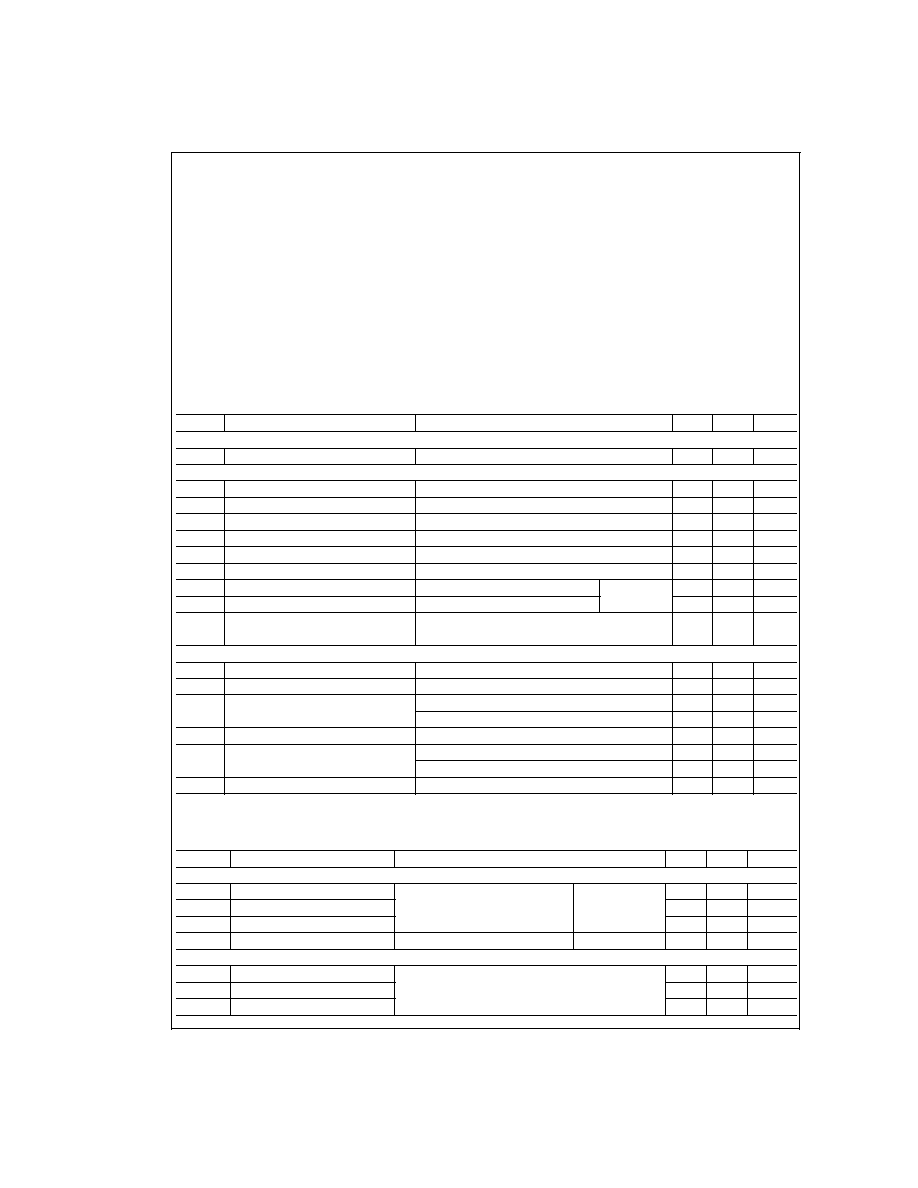
Connection Diagrams
Parameter Measurement Information
J Package
16-Lead Dual-In-line Package
DS010744-1
E Package
20-Lead Ceramic Leadless Chip Carrier
DS010744-10
For Complete Military Product Specifications
See MDS or SMD.
Order Number DS14C232J/883 or DS14C232E/883
See NS Package Number E20A or J16A
DS010744-3
FIGURE 1. Driver Load Circuit
DS010744-4
FIGURE 2. Driver Switching Waveform
DS14C232
www.national.com
5