DS26LV31T
3V Enhanced CMOS Quad Differential Line Driver
General Description
The DS26LV31T is a high-speed quad differential CMOS
driver that meets the requirements of both TIA/EIA-422-B
and ITU-T V.11. The CMOS DS26LV31T features low static
I
CC
of 100 µA MAX which makes it ideal for battery powered
and power conscious applications.
Differential outputs have the same V
OD
guarantee (
2V) as
the 5V version.
The EN and EN* inputs allow active Low or active High con-
trol of the TRI-STATE
Æ
outputs. The enables are common to
all four drivers. Protection diodes protect all the driver inputs
against electrostatic discharge. Outputs have enhanced
ESD protection providing greater than 7 kV tolerance. The
driver and enable inputs (DI, EN, EN*) are compatible with
low voltage LVTTL and LVCMOS devices.
Features
n
Industrial product meets TIA/EIA-422-B (RS-422) and
ITU-T V.11 recommendation
n
Military product conforms to TIA/EIA-422-B (RS-422)
n
Interoperable with existing 5V RS-422 networks
n
Industrial and Military temperature range
n
Guaranteed V
OD
of 2V min over operating conditions
n
Balanced output crossover for low EMI (typical within
40 mV of 50% voltage level)
n
Low power design (330 µW 3.3V static)
n
ESD
7 kV on cable I/O pins (HBM)
n
Guaranteed AC parameter:
-- Maximum driver skew:
2 ns
-- Maximum transition time:
10 ns
n
Pin compatible with DS26C31
n
Available in SOIC and Cerpack packaging
n
Standard Microcircuit Drawing (SMD) 5962-98584
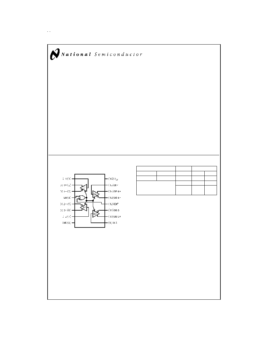
Connection Diagram
Truth Table
Enables
Input
Outputs
EN
EN*
DI
DO+
DO-
L
H
X
Z
Z
All other
combinations of
enable inputs
L
L
H
H
H
L
L = Low logic state
X = Irrelevant
H = High logic state
Z = TRI-STATE
TRI-STATE
Æ
is a registered trademark of National Semiconductor Corporation.
Dual-In-Line Package
DS012642-1
Top View
Order Number DS26LV31TM or DS26LV31W
See NS Package Number M16A or W16A
March 1999
DS26L
V31T
3V
Enhanced
CMOS
Quad
Differential
Line
Driver
© 1999 National Semiconductor Corporation
DS012642
www.national.com

Absolute Maximum Ratings
(Note 1)
If Military/Aerospace specified devices are required,
please contact the National Semiconductor Sales Office/
Distributors for availability and specifications.
Supply Voltage (V
CC
)
-0.5V to +7V
Enable Input Voltage (EN, EN*)
-0.5V to V
CC
+ 0.5V
Driver Input Voltage (DI)
-0.5V to V
CC
+ 0.5V
Clamp Diode Current
±
20 mA
DC Output Current, per pin
±
150 mA
Driver Output Voltage
(Power Off: DO+, DO-)
-0.5V to +7V
Maximum Package Power Dissipaton +25∞C
M Package
1226 mW
W Package
1119 mW
Derate M Package 9.8 mW/∞C above +25∞C
Derate W Package 7.5 mW/∞C above +25∞C
Storage Temperature Range
-65∞C to +150∞C
Lead Temperature Range
Soldering
(4 sec.)
+260∞C
ESD Ratings (HBM, 1.5 k
, 100
pF)
Driver Outputs
7 kV
Other Pins
2.5 kV
Recommended Operating
Conditions
Min
Typ
Max
Units
Supply Voltage (V
CC
)
3.0
3.3
3.6
V
Operating Free Air Temperature Range (T
A
)
DS26LV31T
-40
+25
+85
∞C
DS26LV31W
-55
+25
+125
∞C
Input Rise and Fall Time
500
ns
Electrical Characteristics
(Note 2) (Note 3)
Over supply voltage and operating temperature ranges, unless otherwise specified
Symbol
Parameter
Conditions
Pin
Min
Typ
Max
Units
V
OD1
Output Differential Voltage
R
L
=
(No Load)
DO+,
3.3
4
V
V
OD2
Output Differential Voltage
R
L
= 100
(
Figure 1)
DO-
2
2.6
V
V
OD2
Change in Magnitude of
I
O
20 mA
-400
7
400
mV
Output Differential Voltage
V
OD3
Output Differential Voltage
R
L
= 3900
(V.11)
Figure 1 (Note 7)
3.2
3.6
V
V
OC
Common Mode Voltage
R
L
= 100
(
Figure 1)
1.5
2
V
V
OC
Change in Magnitude of
-400
6
400
mV
Common Mode Voltage
I
OZ
TRI-STATE Leakage
V
OUT
= V
CC
or GND
±
0.5
±
20
µA
Current
Drivers Disabled
I
SC
Output Short Circuit Currrent
V
OUT
= 0V
V
IN
= V
CC
or
GND (Note 4)
T
A
= -40∞C to
+85∞C
-40
-70
-150
mA
T
A
= -55∞C to
+125∞C (Note
10)
-30
-160
mA
I
OFF
Output Leakage Current
V
CC
= 0V, V
OUT
= 3V or 6V
0.03
100
µA
V
CC
= 0V, V
OUT
= -0.25V
T
A
= -40∞C to
+85∞C
-0.08
-100
µA
T
A
= -55∞C to
+125∞C
-200
µA
V
IH
High Level Input Voltage
DI,
2.0
V
CC
V
V
IL
Low Level Input Voltage
EN,
GND
0.8
V
I
IH
High Level Input Current
V
IN
= V
CC
EN*
10
µA
I
IL
Low Level Input Current
V
IN
= GND
-10
µA
V
CL
Input Clamp Voltage
I
IN
= -18 mA
-1.5
V
I
CC
Power Supply Current
No Load, V
IN
(all) = V
CC
or
GND
T
A
= -40∞C to
+85∞C
V
CC
100
µA
T
A
= -55∞C to
+125∞C
125
µA
www.national.com
2

Switching Characteristics - Industrial
(Note 5) (Note 6)
Over supply voltage and -40∞C to +85∞C operating temperature range, unless otherwise specified
Sym
Parameter
Conditions
Min
Typ
Max
Units
t
PHLD
Differential Propagation Delay
R
L
= 100
, C
L
= 50 pF
6
10.5
16
ns
High to Low
(
Figures 2, 3)
t
PLHD
Differential Propagation Delay
6
11
16
ns
Low to High
t
SKD
Differential Skew (same
0.5
2.0
ns
channel) |t
PHLD
- t
PLHD
|
t
SK1
Skew, Pin to Pin
1.0
2.0
ns
(same device)
t
SK2
Skew, Part to Part (Note 8)
3.0
5.0
ns
t
TLH
Differential Transition Time
4.2
10
ns
Low to High (20% to 80%)
t
THL
Differential Transition Time
4.7
10
ns
High to Low (80% to 20%)
t
PHZ
Disable Time High to Z
(
Figures 4, 5)
12
20
ns
t
PLZ
Disable Time Low to Z
9
20
ns
t
PZH
Enable Time Z to High
22
32
ns
t
PZL
Enable Time Z to Low
22
32
ns
f
max
Maximum Operating
32
MHz
Frequency (Note 9)
Switching Characteristics - Military
(Note 5) (Note 6)
Over supply voltage and -55∞C to +125∞C operating temperature range, unless otherwise specified
Sym
Parameter
Conditions
Min
Max
Units
t
PHLD
Differential Propagation Delay
R
L
= 100
, C
L
= 50 pF
5
25
ns
High to Low
(
Figures 2, 3)
t
PLHD
Differential Propagation Delay
5
25
ns
Low to High
t
SKD
Differential Skew (same
5.0
ns
channel) |t
PHLD
- t
PLHD
|
t
SK1
Skew, Pin to Pin
5.0
ns
(same device)
t
PHZ
Disable Time High to Z
(
Figures 4, 5)
35
ns
t
PLZ
Disable Time Low to Z
35
ns
t
PZH
Enable Time Z to High
40
ns
t
PZL
Enable Time Z to Low
40
ns
Note 1: "Absolute Maximum Ratings" are those values beyond which the safety of the device cannot be guaranteed. They are not meant to imply that the devices
should be operated at these limits. The table of "Electrical Characteristics" specifies conditions of device operation.
Note 2: Current into device pins is defined as positive. Current out of device pins is defined as negative. All voltages are referenced to ground except differential volt-
ages V
OD1
, V
OD2
, V
OD3
.
Note 3: All typicals are given for V
CC
= +3.3V, T
A
= +25∞C.
Note 4: Only one output shorted at a time. The output (true or complement) is configured High.
Note 5: f = 1 MHz, t
r
and t
f
6 ns, 10% to 90%.
Note 6: See TIA/EIA-422-B specifications for exact test conditions.
Note 7: This specification limit is for compliance with TIA/EIA-422-B and ITU-T V.11.
Note 8: Devices are at the same V
CC
and within 5∞C within the operating temperature range
Note 9: All channels switching, output duty cycle criteria is 40%/60% measured at 50%. This parameter is guaranteed by design and characterization.
Note 10: This parameter does not meet the TIA/EIA-422-B specification.
www.national.com
3

Parameter Measurement Information
Note 11: Generator waveform for all tests unless otherwise specified: f = 1 MHz, Duty Cycle = 50% Z
o
= 50
, t
r
10 ns, t
f
10.
Note 12: C
L
includes probe and fixture capacitance.
DS012642-2
FIGURE 1. Differential Driver DC Test Circuit
DS012642-3
FIGURE 2. Differential Driver Propagation Delay and Transition Time Test Circuit
DS012642-4
FIGURE 3. Differential Driver Propagation Delay and Transition Time Waveforms
www.national.com
4

Parameter Measurement Information
(Continued)
DS012642-5
If EN is the input, then EN* = High
If EN* is the input, then EN = Low
FIGURE 4. Driver Single-Ended TRI-STATE Test Circuit
DS012642-6
FIGURE 5. Driver Single-Ended TRI-STATE Waveforms
www.national.com
5