 | ÐлекÑÑоннÑй компоненÑ: DS36C280 | СкаÑаÑÑ:  PDF PDF  ZIP ZIP |
Äîêóìåíòàöèÿ è îïèñàíèÿ www.docs.chipfind.ru
DS36C280
Slew Rate Controlled CMOS EIA-RS-485 Transceiver
General Description
The DS36C280 is a low power differential bus/line trans-
ceiver designed to meet the requirements of RS-485 Stan-
dard for multipoint data transmission. In addition, it is com-
patible with TIA/EIA-422-B.
The slew rate control feature allows the user to set the driver
rise and fall times by using an external resistor. Controlled
edge rates can reduce switching EMI.
The CMOS design offers significant power savings over its
bipolar and ALS counterparts without sacrificing ruggedness
against ESD damage. The device is ideal for use in battery
powered or power conscious applications. I
CC
is specified at
500 µA maximum.
The driver and receiver outputs feature TRI-STATE
®
capabil-
ity. The driver outputs operate over the entire common mode
range of -7V to +12V. Bus contention or fault situations are
handled by a thermal shutdown circuit, which forces the
driver outputs into the high impedance state.
The receiver incorporates a fail safe circuit which guarantees
a high output state when the inputs are left open (Note 1) .
Features
n
100% RS-485 compliant
-- Guaranteed RS-485 device interoperation
n
Low power CMOS design:
I
CC
500 µA max
n
Adjustable slew rate control
-- Minimizes EMI affects
n
Built-in power up/down glitch-free circuitry
-- Permits live transceiver insertion/displacement
n
DIP and SOIC packages available
n
Industrial temperature range:
-40°C to +85°C
n
On-board thermal shutdown circuitry
-- Prevents damage to the device in the event of
excessive power dissipation
n
Wide common mode range:
-7V to +12V
n
Receiver open input fail-safe (Note 1)
n
1
/
4
unit load (DS36C280):
128 nodes
n
1
/
2
unit load (DS36C280T):
64 nodes
n
ESD (human body model):
2 kV
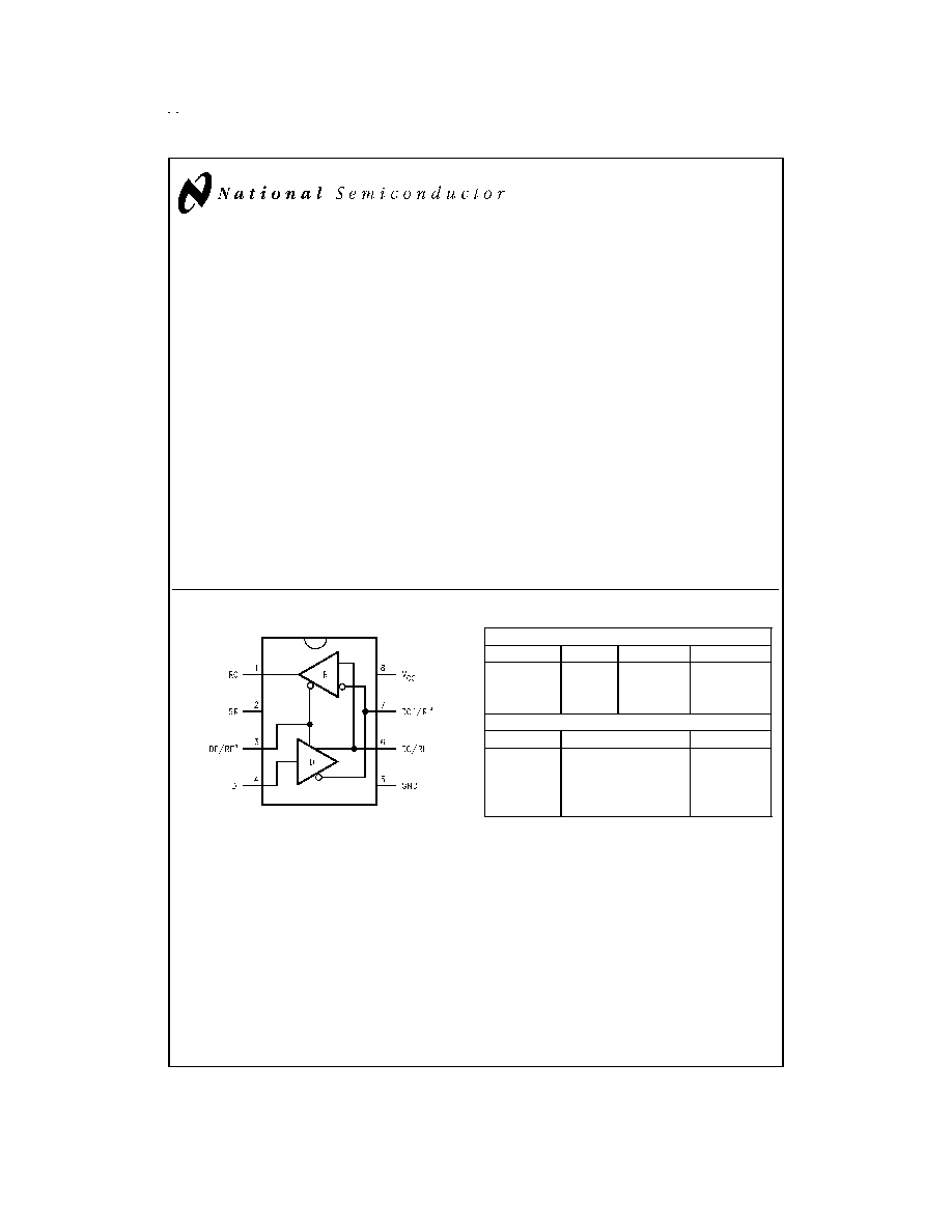
Connection and Logic Diagram
Truth Table
DRIVER SECTION
DE/RE*
DI
DO/RI
DO*/RI*
H
H
H
L
H
L
L
H
L
X
Z
Z
RECEIVER SECTION
DE/RE*
RI-RI*
RO
L
+0.2V
H
L
-0.2V
L
H
X
Z
L
OPEN (Note 1)
H
Note 1: Non-terminated, Open Inputs only
TRI-STATE
®
is a registered trademark of National Semiconductor Corporation.
DS012052-1
Order Number DS36C280TM, DS36C280TN
DS36C280M and DS36C280N
See NS Package Number M08A or N08E
July 1998
DS36C280
Slew
Rate
Controlled
CMOS
EIA-RS-485
T
ransceiver
© 1999 National Semiconductor Corporation
DS012052
www.national.com
Absolute Maximum Ratings
(Note 2)
If Military/Aerospace specified devices are required,
please contact the National Semiconductor Sales Office/
Distributors for availability and specifications.
Supply Voltage (V
CC
)
+12V
Input Voltage (DE/RE*, & DI)
-0.5V to (V
CC
+0.5V)
Common Mode (V
CM
)
Driver Output/Receiver Input
±
15V
Input Voltage (DO/RI, DO*/RI*)
±
14V
Receiver Output Voltage
-0.5V to (V
CC
+0.5V)
Maximum Package Power Dissipation
@
+25°C
M Package 1190 mV, derate
9.5 mW/°C above +25°C
N Package 794 mV, derate
6.0 mW/°C above +25°C
Storage Temperature Range
-65°C to +150°C
Lead Temperature
+260°C
(Soldering 4 sec.)
Recommended Operating
Conditions
Min
Typ
Max
Units
Supply Voltage (V
CC
)
+4.75
+5.0
+5.25
V
Bus Voltage
-7
+12
V
Operating Free Air Temperature (T
A
)
DS36C280T
-40
+25
+85
°C
DS36C280
0
+25
+70
°C
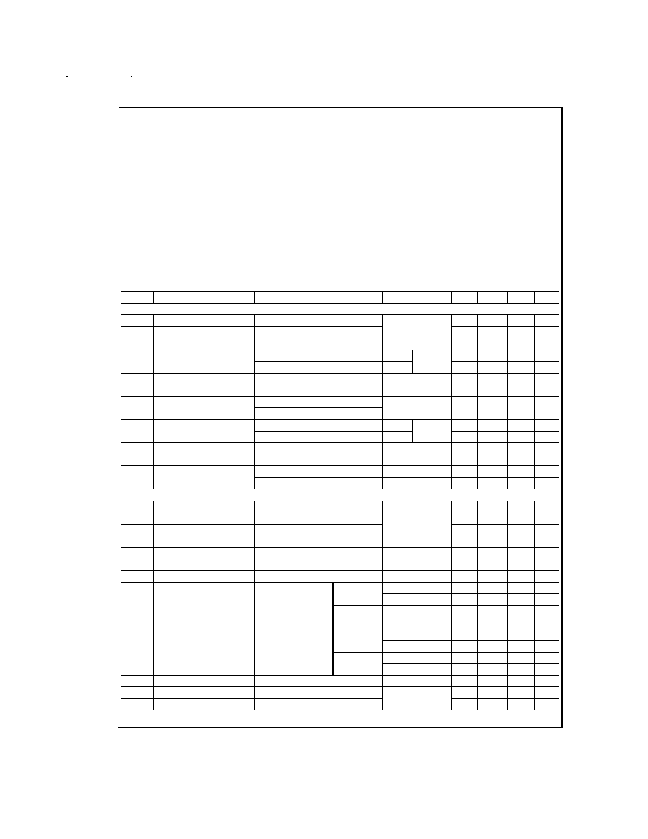
Electrical Characteristics
(Notes 3, 4)
Over Supply Voltage and Operating Temperature ranges, unless otherwise specified
Symbol
Parameter
Conditions
Reference
Min
Typ
Max
Units
DIFFERENTIAL DRIVER CHARACTERISTICS
V
OD1
Differential Output Voltage
I
O
= 0 mA (No Load)
(422)
(485)
1.5
5.0
V
V
OD0
Output Voltage
I
O
= 0 mA
0
5.0
V
V
OD0*
Output Voltage
(Output to GND)
0
5.0
V
V
OD2
Differential Output Voltage
(Termination Load)
R
L
= 50
(422)
Figure 1
2.0
2.8
V
R
L
= 27
(485)
1.5
2.3
5.0
V
V
OD2
Balance of V
OD2
R
L
= 27
or 50
(Note 5)
-0.2
0.1
+0.2
V
|V
OD2
- V
OD2*
|
(422, 485)
V
OD3
Differential Output Voltage
(Full Load)
R1 = 54
, R2 = 375
Figure 2
1.5
2.0
5.0
V
V
TEST
= -7V to +12V
V
OC
Driver Common Mode
Output Voltage
R
L
= 27
(485)
Figure 1
0
3.0
V
R
L
= 50
(422)
0
3.0
V
V
OC
Balance of V
OC
R
L
= 27
or
(Note 5)
-0.2
+0.2
V
|V
OC
- V
OC*
|
R
L
= 50
(422, 485)
I
OSD
Driver Output Short-Circuit
Current
V
O
= +12V
(485)
Figure 4
200
+250
mA
V
O
= -7V
(485)
-190
-250
mA
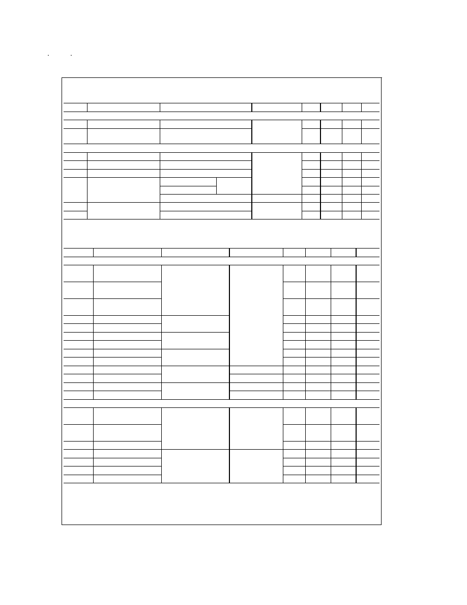
RECEIVER CHARACTERISTICS
V
TH
Differential Input High
Threshold Voltage
V
O
= V
OH
, I
O
= -0.4 mA
(Note 6)
(422, 485)
+0.035
+0.2
V
-7V
V
CM
+12V
V
TL
Differential Input Low
Threshold Voltage
V
O
= V
OL
, I
O
= 0.4 mA
-0.2
-0.035
V
-7V
V
CM
+12V
V
HST
Hysteresis
V
CM
= 0V
70
mV
R
IN
Input Resistance
-7V
V
CM
+12V
DS36C280T
24
68
k
R
IN
Input Resistance
-7V
V
CM
+12V
DS36C280
48
68
k
I
IN
Line Input Current
(Note 8)
Other Input = 0V
DS36C280
V
IN
= +12V
0
0.19
0.25
mA
DE = V
IL
, RE* = V
IL
V
IN
= -7V
0
-0.1
-0.2
mA
V
CC
= 4.75 to 5.25
DS36C280T
V
IN
= +12V
0
0.19
0.5
mA
or 0V
V
IN
= -7V
0
-0.1
-0.4
mA
I
ING
Line Input Current
Glitch (Note 8)
Other Input = 0V
DS36C280
V
IN
= +12V
0
0.19
0.25
mA
DE = V
IL
, RE* = V
IL
V
IN
= -7V
0
-0.1
-0.2
mA
V
CC
= +3.0V
DS36C280T
V
IN
= +12V
0
0.19
0.5
mA
or 0V T
A
= 25°C
V
IN
= -7V
0
-0.1
-0.4
mA
I
B
Input Balance Test
RS = 500
(422) (Note 10)
±
400
mV
V
OH
High Level Output Voltage
I
OH
= -4 mA, V
ID
= +0.2V
RO
Figure 11
3.5
4.6
V
V
OL
Low Level Output Voltage
I
OL
= +4 mA, V
ID
= -0.2V
0.3
0.5
V
www.national.com
2
Electrical Characteristics
(Notes 3, 4) (Continued)
Over Supply Voltage and Operating Temperature ranges, unless otherwise specified
Symbol
Parameter
Conditions
Reference
Min
Typ
Max
Units
RECEIVER CHARACTERISTICS
I
OSR
Short Circuit Current
V
O
= GND
RO
7
35
85
mA
I
OZR
TRI-STATE Leakage
Current
V
O
= 0.4V to 2.4V
±
1
µA
DEVICE CHARACTERISTICS
V
IH
High Level Input Voltage
DE/RE*,
DI
2.0
V
CC
V
V
IL
Low Level Input Voltage
GND
0.8
V
I
IH
High Level Input Current
V
IH
= V
CC
2
µA
I
IL
Low Level Input Current
V
CC
= 5.0V
V
IL
= 0V
-2
µA
V
CC
= +3.0V
-2
µA
SR = 0V
SR
-1
mA
I
CCR
Power Supply Current
(No Load)
Driver OFF, Receiver ON
V
CC
200
500
µA
I
CCD
Driver ON, Receiver OFF
200
500
µA
Switching Characteristics
(Notes 4, 9, 11)
Over Supply Voltage and Operating Temperature ranges, unless otherwise specified
Symbol
Parameter
Conditions
Reference
Min
Typ
Max
Units
DRIVER CHARACTERISTICS
t
PHLD
Differential Propagation
Delay High to Low
R
L
= 54
, C
L
= 100 pF
Figures 5, 6
10
399
1000
ns
t
PLHD
Differential Propagation
Delay Low to High
10
400
1000
ns
t
SKD
Differential Skew
0
1
10
ns
|t
PHLD
- t
PLHD
|
t
r
Rise Time
SR = Open
2870
ns
t
f
Fall Time
3070
ns
t
r
Rise Time
SR = 100 k
1590
ns
t
f
Fall Time
1640
ns
t
r
Rise Time
SR = Short
100
337
1000
ns
t
f
Fall Time
100
348
1000
ns
t
PHZ
Disable Time High to Z
C
L
= 15 pF
Figures 7, 8
1100
2000
ns
t
PLZ
Disable Time Low to Z
Figures 9, 10
500
800
ns
t
PZH
Enable Time Z to High
C
L
= 100 pF
Figures 7, 8
300
500
ns
t
PZL
Enable Time Z to Low
Figures 9, 10
300
500
ns
RECEIVER CHARACTERISTICS
t
PHL
Propagation Delay
High to Low
C
L
= 15 pF
Figures 12, 13
30
210
400
ns
t
PLH
Propagation Delay
Low to High
30
190
400
ns
t
SK
Skew, |t
PHL
- t
PLH
|
0
20
50
ns
t
PLZ
Output Disable Time
C
L
= 15 pF
Figures 14, 15, 16
50
150
ns
t
PHZ
55
150
ns
t
PZL
Output Enable Time
40
150
ns
t
PZH
45
150
ns
Note 2: "Absolute Maximum Ratings" are those values beyond which the safety of the device cannot be guaranteed. They are not meant to imply that the devices
should be operated at these limits. The table of "Electrical Characteristics" specifies conditions of device operation.
Note 3: Current into device pins is defined as positive. Current out of device pins is defined as negative. All voltages are referenced to ground except V
OD1
and V
OD2
.
Note 4: All typicals are given for: V
CC
= +5.0V, T
A
= + 25°C.
Note 5: Delta |V
OD2
| and Delta |V
OC
| are changes in magnitude of V
OD2
and V
OC
, respectively, that occur when input changes state.
www.national.com
3
Switching Characteristics
(Notes 4, 9, 11) (Continued)
Note 6: Threshold parameter limits specified as an algebraic value rather than by magnitude.
Note 7: Hysteresis defined as V
HST
= V
TH
- V
TL
.
Note 8: I
IN
includes the receiver input current and driver TRI-STATE leakage current.
Note 9: C
L
includes probe and jig capacitance.
Note 10: For complete details of test, see RS-485.
Note 11: SR = GND for all Switching Characteristics unless otherwise specified.
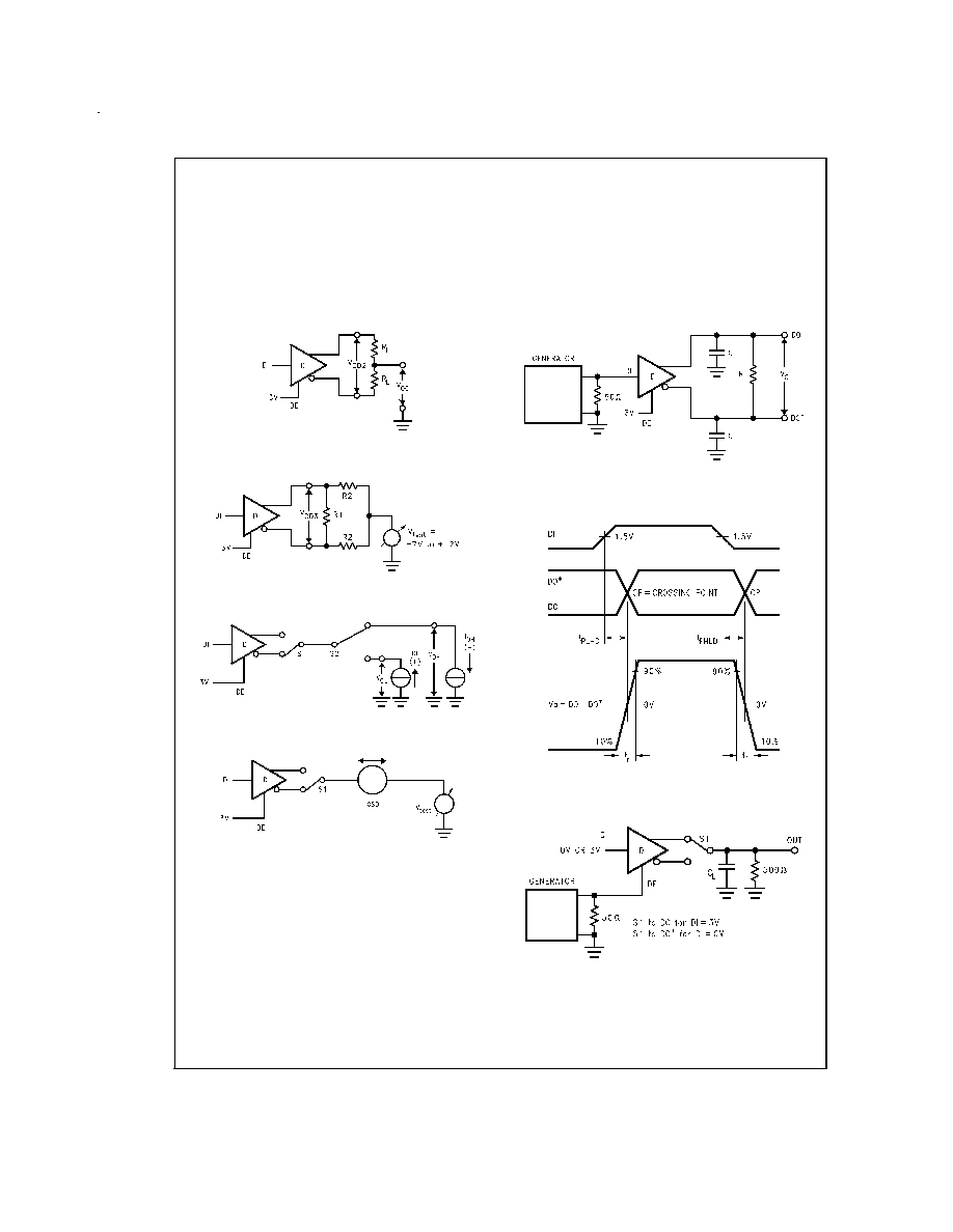
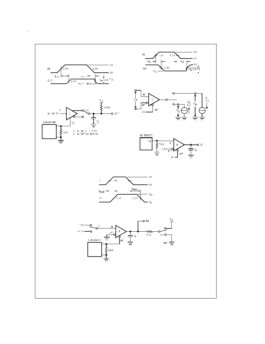
Parameter Measurement Information
DS012052-2
FIGURE 1. Driver V
OD2
and V
OC
DS012052-18
FIGURE 2. Driver V
OD3
DS012052-3
FIGURE 3. Driver V
OH
and V
OL
DS012052-4
Vtest = -7V to +12V
FIGURE 4. Driver I
OSD
DS012052-5
FIGURE 5. Driver Differential
Propagation Delay Test Circuit
DS012052-6
FIGURE 6. Driver Differential Propagation Delays
and Differential Rise and Fall Times
DS012052-7
FIGURE 7. TRI-STATE Test Circuit (t
PZH
, t
PHZ
)
www.national.com
4
Parameter Measurement
Information
(Continued)
DS012052-8
FIGURE 8. TRI-STATE Waveforms (t
PZH
, t
PHZ
)
DS012052-9
FIGURE 9. TRI-STATE Test Circuit (t
PZL
, t
PLZ
)
DS012052-10
FIGURE 10. TRI-STATE Waveforms (t
PZL
, t
PLZ
)
DS012052-11
FIGURE 11. Receiver V
OH
and V
OL
DS012052-12
FIGURE 12. Receiver Differential
Propagation Delay Test Circuit
DS012052-13
FIGURE 13. Receiver Differential Propagation Delay Waveforms
DS012052-14
FIGURE 14. Receiver TRI-STATE Test Circuit
www.national.com
5