 | –≠–ª–µ–∫—Ç—Ä–æ–Ω–Ω—ã–π –∫–æ–º–ø–æ–Ω–µ–Ω—Ç: DS485TM | –°–∫–∞—á–∞—Ç—å:  PDF PDF  ZIP ZIP |
DS485
Low Power RS-485/RS-422 Multipoint Transceiver
General Description
The DS485 is a low-power transceiver for RS-485 and
RS-422 communication. The device contains one driver and
one receiver. The drivers slew rate allows for operation up to
2.5 Mbps (see Applications Information section).
The transceiver draws 200 µA of supply current when un-
loaded or fully loaded with the driver disabled and operates
from a single +5V supply.
The driver is short-circuit current limited and is protected
against excessive power dissipation by thermal shutdown
circuitry that places the driver outputs into TRI-STATE
Æ
(High Impedance state) under fault conditions. The driver
guarantees a minimum of 1.5V differential output voltage
with maximum loading across the common mode range
(V
OD3
).
The receiver has a failsafe feature that guarantees a
logic-high output if the input is open circuit.
The DS485 is available in surface mount and DIP packages
and is characterized for Industrial and Commercial tempera-
ture range operation.
Features
n
Meets TIA/EIA RS-485 multipoint standard
n
Guaranteed full load output voltage (V
OD3
)
n
Low quiescent current:
200 µA typ
n
-7V to +12V common-mode input voltage range
n
TRI-STATE outputs on driver and receiver
n
AC performance:
-- Driver transition time:
25 ns typ
-- Driver propagation delay:
40 ns typ
-- Driver skew:
1 ns typ
-- Receiver propagation delay:
200 ns typ
-- Receiver skew:
20 ns typ
n
Half-duplex flow through pinout
n
Operates from a single 5V supply
n
Allows up to 32 transceivers on the bus
n
Current-limiting and thermal shutdown for driver
overload protection
n
Industrial temperature range operation
n
Pin and functional compatible with MAX485 and LTC485
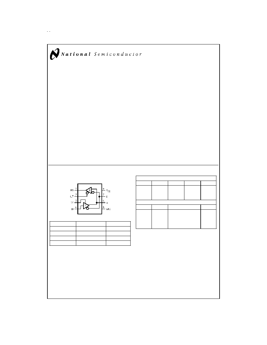
Connection and Logic Diagram
Order Number
Temp. Range
Package/###
DS485N
0∞C to +70∞C
DIP/N08E
DS485M
0∞C to +70∞C
SOP/M08A
DS485TN
-40∞C to +85∞C
DIP/N08E
DS485TM
-40∞C to +85∞C
SOP/M08A
Truth Table
DRIVER SECTION
RE
*
DE
DI
A
B
X
H
H
H
L
X
H
L
L
H
X
L
X
Z
Z
RECEIVER SECTION
RE
*
DE
A-B
RO
L
L
+0.2V
H
L
L
-0.2V
L
H
X
X
Z
L
L
OPEN
*
H
*
Note: Non Terminated, Open Input only
X = indeterminate
Z = TRI-STATE
TRI-STATE
Æ
is a registered trademark of National Semiconductor Corporation.
DIP and SOIC
DS012880-1
July 1998
DS485
Low
Power
RS-485/RS-422
Multipoint
T
ransceiver
© 1999 National Semiconductor Corporation
DS012880
www.national.com

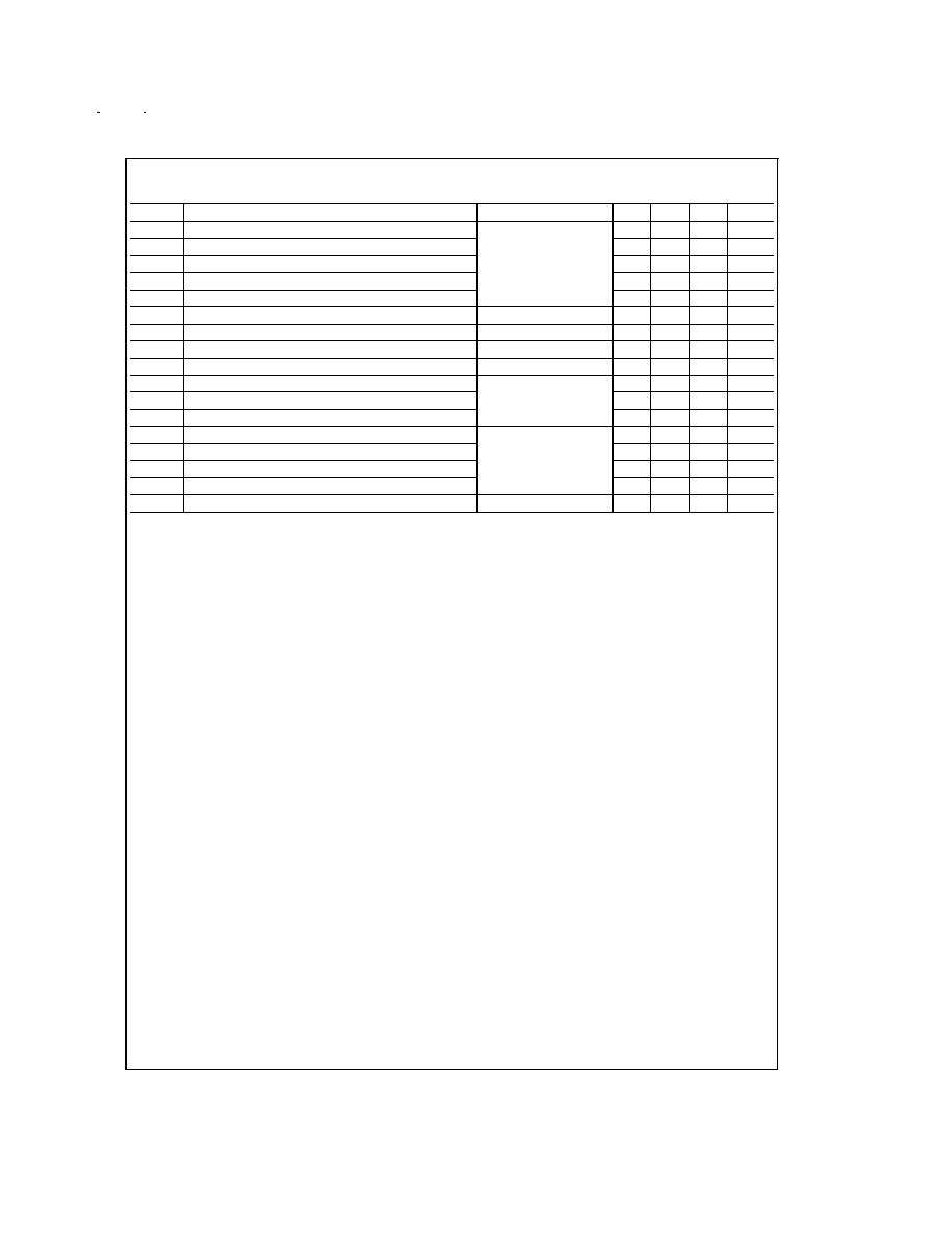
Absolute Maximum Ratings
(Note 1)
If Military/Aerospace specified devices are required,
please contact the National Semiconductor Sales Office/
Distributors for availability and specifications.
Supply Voltage (V
CC
)
+12V
Enable Input Voltage (RE
*
, DE)
-0.5V to (V
CC
+ 0.5V)
Driver Input Voltage (DI)
-0.5V to (V
CC
+ 0.5V)
Driver Output Voltage (A, B)
-14V to +14V
Receiver Input Voltage (A, B)
-14V to +14V
Receiver Output Voltage (RO)
-0.5V to (V
CC
+ 0.5V)
Maximum Package Power Dissipation
@
+25∞C
M Package
1.19W
N Package
0.74W
Derate M Package 9.5 mW/∞C above +25∞C
Derate N Package 6.0 mW/∞C above +25∞C
Maximum Package Power Dissipation
@
+70∞C
M Package
0.76W
N Package
0.47W
Storage Temperature Range
-65∞C to +150∞C
Lead Temperature Range
(Soldering, 4 sec.)
+260∞C
ESD (HBM)
2 kV
Recommended Operating
Conditions
Min
Typ
Max
Units
Supply Voltage (V
CC
)
+4.75
+5.0
+5.25
V
Operating Free Air
Temperature (T
A
)
DS485
0
+25
+70
∞C
DS485T
-40
+25
+85
∞C
Bus Common Mode Voltage
-7
+12
V
Electrical Characteristics
Over Supply Voltage and Operating Temperature Ranges, unless otherwise specified (Notes 2, 3)
Symbol
Parameter
Conditions
Pin
Min
Typ
Max
Units
V
OD1
Differential Driver Output Voltage
(No Load)
A, B
5
V
V
OD2
Differential Driver Output Voltage
R
L
= 50
, (RS422),
Figure 1
2
2.8
V
with Load
R
L
= 27
, (RS485),
Figure 1
1.5
2.3
5
V
V
OD
Change in Magnitude of Output
R
L
= 27
or 50
(Note 4)
0.2
|V|
Differential Voltage
V
OD3
Differential Driver Output Voltage --
R1 = 54
, R2 = 375
1.5
2.0
5
V
Full Load with Max V
CM
V
TEST
= -7V to +12V, Figure 5
V
OC
Driver Common-Mode Output Voltage
R
L
= 27
or 50
,
Figure 1
3
V
V
OC
Change in Magnitude of Common-Mode
R
L
= 27
or 50
,
Figure 1 (Note 4)
0.2
|V|
Output Voltage
V
IH
Input High Voltage
DI,
DE,
RE
*
2.0
V
V
IL
Input Low Voltage
0.8
V
I
IN1
Input Current
V
IN
= 0V or V
CC
±
2
µA
I
IN2
Input Current (Note 5)
V
IN
= +12V
A, B
1.0
mA
DE = 0V, V
CC
= 0V or 5.25V
V
IN
= -7V
-0.8
mA
V
TH
Receiver Differential Threshold Voltage
-7V
V
CM
+12V
-0.2
0.2
V
V
TH
Receiver Input Hysteresis
V
CM
= 0V
70
mV
V
OH
Receiver Output High Voltage
I
O
= -4 mA, V
ID
= 0.2V
RO
3.5
V
V
OL
Receiver Output Low Voltage
I
O
= 4 mA, V
ID
= -0.2V
0.4
V
I
OZR
TRI-STATE Output Current at Receiver
0.4V
V
O
2.4V
±
1
µA
R
IN
Receiver Input Resistance
-7V
V
IN
+12V
A, B
12
k
I
CC
No-Load Supply Current (Note 6)
DE = V
CC
, RE
*
= 0V or V
CC
V
CC
200
900
µA
DE = 0V, RE
*
= 0V or V
CC
200
500
µA
I
OSD1
Driver Short Circuit Current, V
O
= HIGH
-7V
V
O
+12V
A, B
35
250
mA
I
OSD2
Driver Short Circuit Current, V
O
= LOW
-7V
V
O
+12V
35
250
mA
I
OSR
Receiver Short Circuit Current
0V
V
O
V
CC
RO
7
85
mA
www.national.com
2
Switching Characteristics
Over Supply Voltage and Operating Temperature Ranges, unless otherwise specified (Notes 3, 7, 8)
Symbol
Parameter
Conditions
Min
Typ
Max
Units
t
PLHD
Driver Differential Propagation Delay -- Low to High
R
L
= 54
, C
L
= 100 pF
10
40
65
ns
t
PHLD
Driver Differential Propagation Delay -- High to Low
10
39
65
ns
t
SKEW
Differential Skew |t
PHLD
- t
PLHD
|
1
10
ns
t
r
Driver Rise Time
3
25
40
ns
t
f
Driver Fall Time
3
25
40
ns
t
ZH
Driver Enable to Output High
C
L
= 100 pF
170
ns
t
ZL
Driver Enable to Output Low
C
L
= 100 pF
170
ns
t
LZ
Driver Disable from Output Low
C
L
= 15 pF
170
ns
t
HZ
Driver Disable from Output High
C
L
= 15 pF
170
ns
t
PLHD
Receiver Differential Propagation Delay -- Low to High
C
L
= 15 pF (RO)
70
190
320
ns
t
PHLD
Receiver Differential Propagation Delay -- High to Low
70
210
320
ns
t
SKEW
Differential Skew |t
PHLD
- t
PLHD
|
20
50
ns
t
ZH
Receiver Enable to Output High
C
L
= 15 pF
110
ns
t
ZL
Receiver Enable to Output Low
110
ns
t
LZ
Receiver Disable from Output Low
110
ns
t
HZ
Receiver Disable from Output High
110
ns
f
max
Maximum Data Rate
(Note 9)
2.5
Mbps
Note 1: "Absolute Maximum Ratings" are those values beyond which the safety of the device cannot be guaranteed. They are not meant to imply that the devices
should be operated at these limits. The table of "Electrical Characteristics" specifies conditions of device operation.
Note 2: Current into device pins is defined as positive. Current out of device pins is defined as negative. All voltages are referenced to ground except V
OD1/2/3
and
V
ID
.
Note 3: All typicals are given for: V
CC
= +5.0V, T
A
= +25∞C.
Note 4:
|V
OD
| and
|V
OC
| are changes in magnitude of V
OD
and V
OC
respectively, that occur when the input changes state.
Note 5: I
IN2
includes the receiver input current and driver TRI-STATE leakage current.
Note 6: Supply current specification is valid for loaded transmitters when DE = 0V or enabled (DE = H) with no load.
Note 7: f = 1 MHz, t
r
and t
f
6 ns, Z
O
= 50
.
Note 8: C
L
includes jig and probe capacitance.
Note 9: f
max
is the guaranteed data rate for 50 ft of twisted pair cable. f
max
may be conservatively determined from the ratio of driver transition time (t
r
) to the data
rate unit interval (1/f
max
). Using a 10% ratio yields f
max
= (0.1)/40 ns = 2.5 Mb/s. Higher data rates may be supported by allowing larger ratios.
www.national.com
3
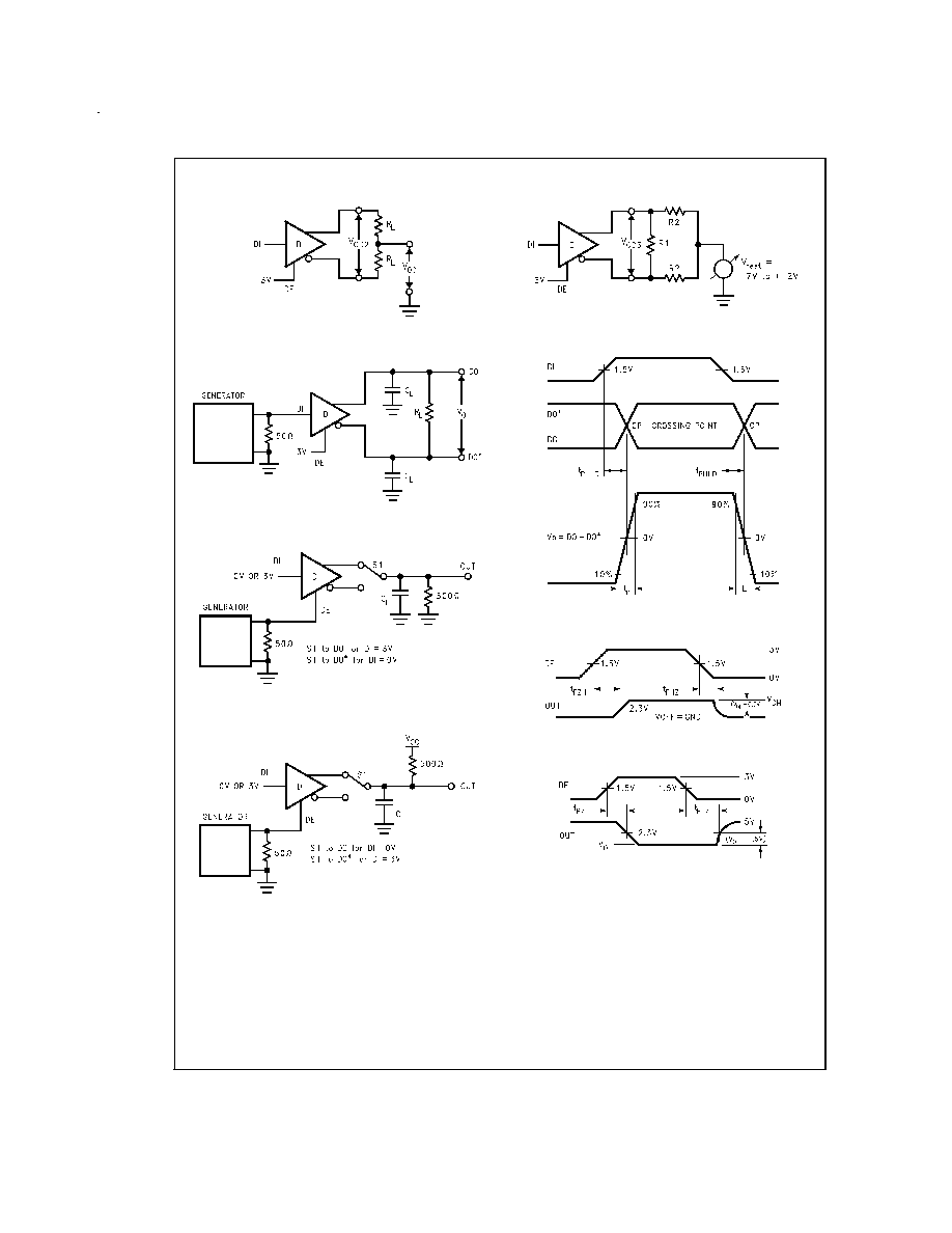
Parameter Measurement Information
DS012880-2
FIGURE 1. V
OD
DS012880-4
FIGURE 2.
DS012880-6
FIGURE 3.
DS012880-8
FIGURE 4.
DS012880-3
FIGURE 5. V
OD3
DS012880-5
FIGURE 6.
DS012880-7
FIGURE 7.
DS012880-9
FIGURE 8.
www.national.com
4
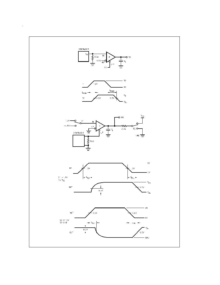
Parameter Measurement Information
(Continued)
DS012880-10
FIGURE 9.
DS012880-11
FIGURE 10.
DS012880-12
FIGURE 11.
DS012880-13
FIGURE 12.
DS012880-14
FIGURE 13.
www.national.com
5