 | –≠–Ľ–Ķ–ļ—ā—Ä–ĺ–Ĺ–Ĺ—č–Ļ –ļ–ĺ–ľ–Ņ–ĺ–Ĺ–Ķ–Ĺ—ā: DS75176 | –°–ļ–į—á–į—ā—Ć:  PDF PDF  ZIP ZIP |
DS75176B/DS75176BT
Multipoint RS-485/RS-422 Transceivers
General Description
The DS75176B is a high speed differential TRI-STATE
ģ
bus/line transceiver designed to meet the requirements of
EIA standard RS485 with extended common mode range
(+12V to -7V), for multipoint data transmission. In addition, it
is compatible with RS-422.
The driver and receiver outputs feature TRI-STATE capabil-
ity, for the driver outputs over the entire common mode
range of +12V to -7V. Bus contention or fault situations that
cause excessive power dissipation within the device are
handled by a thermal shutdown circuit, which forces the
driver outputs into the high impedance state.
DC specifications are guaranteed over the 0 to 70įC tem-
perature and 4.75V to 5.25V supply voltage range.
Features
n
Meets EIA standard RS485 for multipoint bus
transmission and is compatible with RS-422.
n
Small Outline (SO) Package option available for
minimum board space.
n
22 ns driver propagation delays.
n
Single +5V supply.
n
-7V to +12V bus common mode range permits
Ī
7V
ground difference between devices on the bus.
n
Thermal shutdown protection.
n
High impedance to bus with driver in TRI-STATE or with
power off, over the entire common mode range allows
the unused devices on the bus to be powered down.
n
Pin out compatible with DS3695/A and SN75176A/B.
n
Combined impedance of a driver output and receiver
input is less than one RS485 unit load, allowing up to 32
transceivers on the bus.
n
70 mV typical receiver hysteresis.
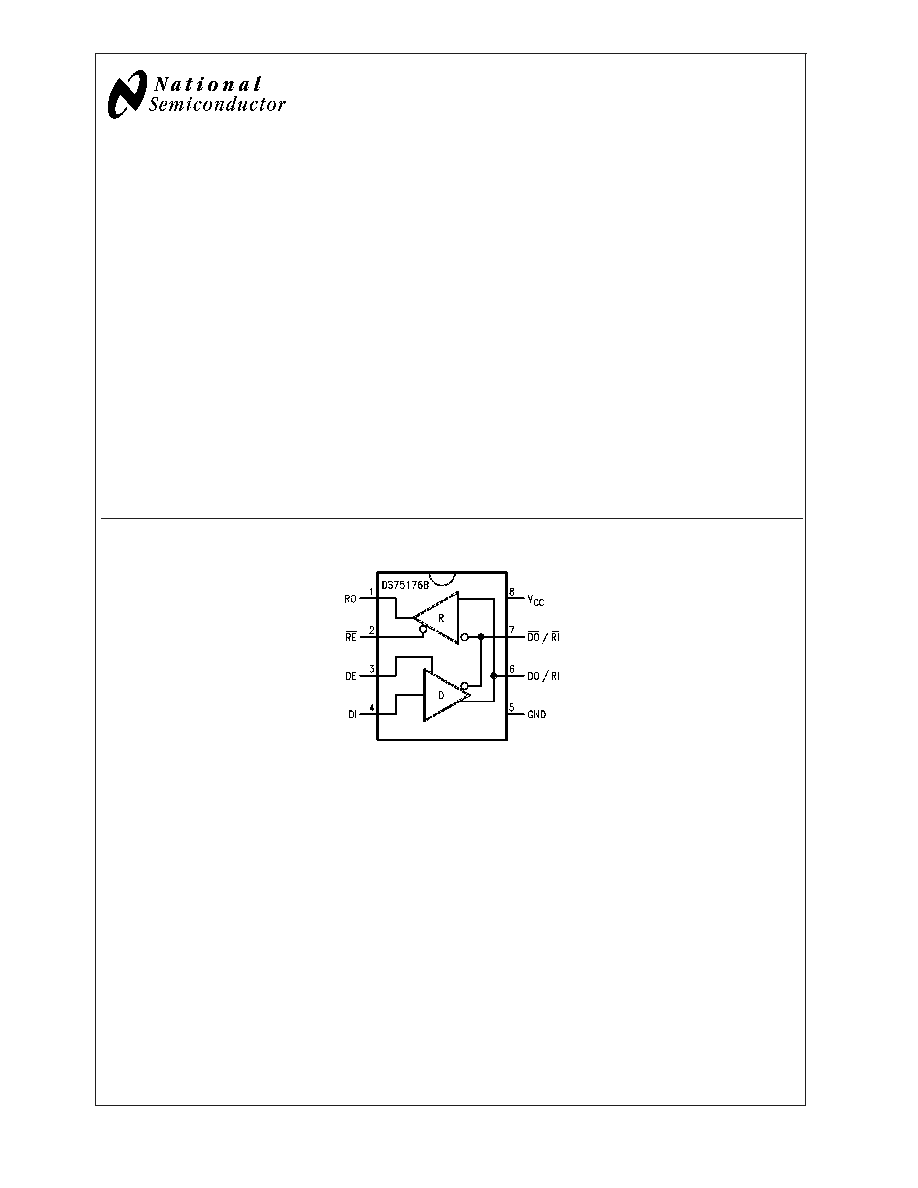
Connection and Logic Diagram
00875901
Top View
Order Number DS75176BN, DS75176BTN, DS75176BM or DS75176BTM
See NS Package Number N08E or M08A
TRI-STATE
ģ
is a registered trademark of National Semiconductor Corp.
July 2004
DS75176B/DS75176BT
Multipoint
RS-485/RS-422
T
ransceivers
© 2004 National Semiconductor Corporation
DS008759
www.national.com

Absolute Maximum Ratings
(Note 1)
If Military/Aerospace specified devices are required,
please contact the National Semiconductor Sales Office/
Distributors for availability and specifications.
Supply Voltage, V
CC
7V
Control Input Voltages
7V
Driver Input Voltage
7V
Driver Output Voltages
+15V/ -10V
Receiver Input Voltages (DS75176B)
+15V/ -10V
Receiver Output Voltage
5.5V
Continuous Power Dissipation
@
25įC
for M Package
675 mW (Note 5)
for N Package
900 mW (Note 4)
Storage Temperature Range
-65įC to +150įC
Lead Temperature
(Soldering, 4 seconds)
260įC
ESD Rating (HBM)
500V
Recommended Operating
Conditions
Min
Max Units
Supply Voltage, V
CC
4.75 5.25
V
Voltage at Any Bus Terminal
-7
+12
V
(Separate or Common Mode)
Operating Free Air Temperature T
A
DS75176B
0
+70
įC
DS75176BT
-40
+85
įC
Differential Input Voltage,
VID (Note 6)
-12
+12
V
Electrical Characteristics
(Notes 2, 3)
0įC
T
A
70įC, 4.75V
<
V
CC
<
5.25V unless otherwise specified
Symbol
Parameter
Conditions
Min Typ Max
Units
V
OD1
Differential Driver Output
I
O
= 0
5
V
Voltage (Unloaded)
V
OD2
Differential Driver Output
(Figure 1)
R = 50
; (RS-422) (Note 7)
2
V
Voltage (with Load)
R = 27
; (RS-485)
1.5
V
V
OD
Change in Magnitude of Driver
Differential Output Voltage For
0.2
V
Complementary Output States
V
OC
Driver Common Mode Output
(Figure 1)
R = 27
3.0
V
Voltage
|V
OC
|
Change in Magnitude of Driver
Common Mode Output Voltage
0.2
V
For Complementary Output
States
V
IH
Input High Voltage
2
V
V
IL
Input Low Voltage
DI, DE,
0.8
V
CL
Input Clamp Voltage
RE , E
I
IN
= -18 mA
-1.5
I
IL
Input Low Current
V
IL
= 0.4V
-200
ĶA
I
IH
Input High Current
V
IH
= 2.4V
20
ĶA
I
IN
Input
DO/RI, DO/RI
V
CC
= 0V or 5.25V
V
IN
= 12V
+1.0
mA
Current
DE = 0V
V
IN
= -7V
-0.8
mA
V
TH
Differential Input Threshold
-7V
V
CM
+ 12V
-0.2
+0.2
V
Voltage for Receiver
V
TH
Receiver Input Hysteresis
V
CM
= 0V
70
mV
V
OH
Receiver Output High Voltage
I
OH
= -400 ĶA
2.7
V
V
OL
Output Low Voltage
RO
I
OL
= 16 mA (Note 7)
0.5
V
I
OZR
OFF-State (High Impedance)
V
CC
= Max
Ī
20
ĶA
Output Current at Receiver
0.4V
V
O
2.4V
R
IN
Receiver Input Resistance
-7V
V
CM
+12V
12
k
I
CC
Supply Current
No Load
Driver Outputs Enabled
55
mA
(Note 7)
Driver Outputs Disabled
35
mA
DS75176B/DS75176BT
www.national.com
2
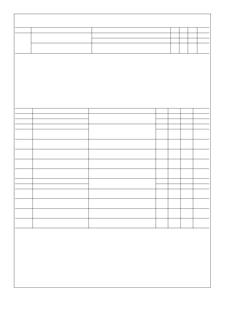
Electrical Characteristics
(Notes 2, 3) (Continued)
0įC
T
A
70įC, 4.75V
<
V
CC
<
5.25V unless otherwise specified
Symbol
Parameter
Conditions
Min Typ Max
Units
I
OSD
Driver Short-Circuit
V
O
= -7V (Note 7)
-250
mA
Output Current
V
O
= +12V (Note 7)
+250
mA
I
OSR
Receiver Short-Circuit
V
O
= 0V
-15
-85
mA
Output Current
Note 1: "Absolute Maximum Ratings" are those beyond which the safety of the device cannot be guaranteed. They are not meant to imply that the device should
be operated at these limits. The tables of "Electrical Characteristics" provide conditions for actual device operation.
Note 2: All currents into device pins are positive; all currents out of device pins are negative. All voltages are referenced to device ground unless otherwise specified.
Note 3: All typicals are given for V
CC
= 5V and T
A
= 25įC.
Note 4: Derate linearly at 5.56 mW/įC to 650 mW at 70įC.
Note 5: Derate linearly @ 6.11 mW/įC to 400 mW at 70įC.
Note 6: Differential - Input/Output bus voltage is measured at the noninverting terminal A with respect to the inverting terminal B.
Note 7: All worst case parameters for which note 7 is applied, must be increased by 10% for DS75176BT. The other parameters remain valid for -40įC
<
T
A
<
+85įC.
Switching Characteristics
V
CC
= 5.0V, T
A
= 25įC
Symbol
Parameter
Conditions
Min
Typ
Max
Units
t
PLH
Driver Input to Output
R
LDIFF
= 60
12
22
ns
t
PHL
Driver Input to Output
C
L1
= C
L2
= 100 pF
17
22
ns
t
r
Driver Rise Time
R
LDIFF
= 60
18
ns
t
f
Driver Fall Time
C
L1
=C
L2
= 100 pF
18
ns
(Figure 3 and Figure 5)
t
ZH
Driver Enable to Output High
C
L
= 100 pF (Figure 4 and Figure 6) S1
Open
29
100
ns
t
ZL
Driver Enable to Output Low
C
L
= 100 pF (Figure 4 and Figure 6) S2
Open
31
60
ns
t
LZ
Driver Disable Time from Low
C
L
= 15 pF (Figure 4 and Figure 6) S2
Open
13
30
ns
t
HZ
Driver Disable Time from High
C
L
= 15 pF (Figure 4 and Figure 6) S1
Open
19
200
ns
t
PLH
Receiver Input to Output
C
L
= 15 pF (Figure 2 and Figure 7)
30
37
ns
t
PHL
Receiver Input to Output
S1 and S2 Closed
32
37
ns
t
ZL
Receiver Enable to Output Low
C
L
= 15 pF (Figure 2 and Figure 8) S2
Open
15
20
ns
t
ZH
Receiver Enable to Output High
C
L
= 15 pF (Figure 2 and Figure 8) S1
Open
11
20
ns
t
LZ
Receiver Disable from Low
C
L
= 15 pF (Figure 2 and Figure 8) S2
Open
28
32
ns
t
HZ
Receiver Disable from High
C
L
= 15 pF (Figure 2 and Figure 8) S1
Open
13
35
ns
DS75176B/DS75176BT
www.national.com
3

AC Test Circuits
Switching Time Waveforms
00875902
FIGURE 1.
00875903
Note: S1 and S2 of load circuit are closed except as otherwise mentioned.
FIGURE 2.
00875904
FIGURE 3.
00875905
Note: Unless otherwise specified the switches are closed.
FIGURE 4.
00875906
FIGURE 5. Driver Propagation Delays and Transition Times
DS75176B/DS75176BT
www.national.com
4
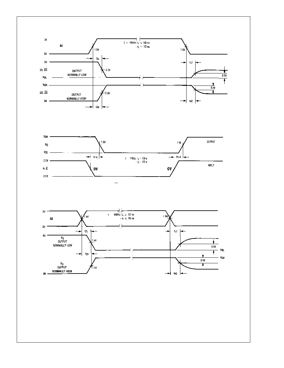
Switching Time Waveforms
(Continued)
00875907
FIGURE 6. Driver Enable and Disable Times
00875908
Note: Differential input voltage may may be realized by grounding RI and pulsing RI between +2.5V and -2.5V
FIGURE 7. Receiver Propagation Delays
00875909
FIGURE 8. Receiver Enable and Disable Times
DS75176B/DS75176BT
www.national.com
5