 | –≠–ª–µ–∫—Ç—Ä–æ–Ω–Ω—ã–π –∫–æ–º–ø–æ–Ω–µ–Ω—Ç: DS90LV019 | –°–∫–∞—á–∞—Ç—å:  PDF PDF  ZIP ZIP |

DS90LV019
3.3V or 5V LVDS Driver/Receiver
General Description
The DS90LV019 is a Driver/Receiver designed specifically
for the high speed low power point-to-point interconnect ap-
plications. The device operates from a single 3.3V or 5.0V
power supply and includes one differential line driver and
one receiver. The DS90LV019 features an independent
driver and receiver with TTL/CMOS compatibility (D
IN
and
R
OUT
). The logic interface provides maximum flexibility as 4
separate lines are provided (D
IN
, DE, RE, and R
OUT
). The
device also features a flow-through pin out which allows
easy PCB routing for short stubs between its pins and the
connector. The driver has 3.5 mA output loop current.
The driver translates between TTL levels (single-ended) to
Low Voltage Differential Signaling levels. This allows for high
speed operation, while consuming minimal power with re-
duced EMI. In addition, the differential signaling provides
common-mode noise rejection.
The receiver threshold is
±
100 mV over a
±
1V common-
mode range and translates the low swing differential levels
to standard (TTL/CMOS) levels.
Features
n
LVDS Signaling
n
3.3V or 5.0V operation
n
Low power CMOS design
n
Balanced Output Impedance
n
Glitch free power up/down (Driver disabled)
n
High Signaling Rate Capacity (above 100 Mbps)
n
Ultra Low Power Dissipation
n
±
1V Common-Mode Range
n
±
100 mV Receiver Sensitivity
n
Product offered in SOIC and TSSOP packages
n
Flow-Through Pin Out
n
Industrial Temperature Range Operation
Connection Diagram
Block Diagram
TRI-STATE
Æ
is a registered trademark of National Semiconductor Corporation.
DS100053-1
Order Number DS90LV019TM or DS90LV019TMTC
See NS Package Number M14A or MTC14
DS100053-2
August 2000
DS90L
V019
3.3V
or
5V
L
VDS
Driver/Receiver
© 2000 National Semiconductor Corporation
DS100053
www.national.com

Absolute Maximum Ratings
(Note 1)
If Military/Aerospace specified devices are required,
please contact the National Semiconductor Sales Office/
Distributors for availability and specifications.
Supply Voltage V
CC
6.0V
Enable Input Voltage (DE, RE)
-0.3V to (V
CC
+0.3V)
Driver Input Voltage (D
IN
)
-0.3V to (V
CC
+ 0.3V)
Receiver Output Voltage
(R
OUT
)
-0.3V to (V
CC
+ 0.3V)
Driver Output Voltage (DO
±
)
-0.3V to +3.9V
Receiver Input Voltage (RI
±
)
-0.3V to (V
CC
+ 0.3V)
Driver Short Circuit Current
Continuous
ESD (Note 4)
(HBM, 1.5 k
, 100 pF)
>
2.0 kV
(EIAJ, 0
, 200 pF)
>
200 V
Maximum Package Power Dissipation at 25∞C
SOIC
960 mW
Derate SOIC Package
7.7mW/∞C
TSSOP
790 mW
Derate TSSOP Package
6.3mW/∞C
Storage Temperature Range
-65∞C to +150∞C
Lead Temperature
(Soldering, 4 sec.)
260∞C
Recommended Operating
Conditions
Min
Max
Units
Supply Voltage (V
CC
) or
3.0
3.6
V
Supply Voltage (V
CC
)
4.5
5.5
V
Receiver Input Voltage
0.0
2.4
V
Operating Free Air
Temperature T
A
-40
+85
∞C
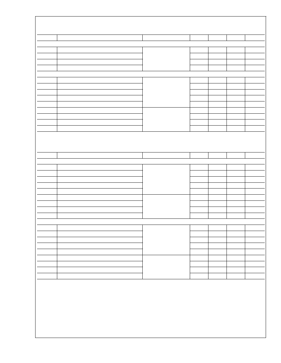
DC Electrical Characteristics
T
A
= -40∞C to +85∞C unless otherwise noted, V
CC
= 3.3
±
0.3V. (Notes 2, 3)
Symbol
Parameter
Conditions
Pin
Min
Typ
Max
Units
DIFFERENTIAL DRIVER CHARACTERISTICS
V
OD
Output Differential Voltage
R
L
= 100
(
Figure 1)
DO+,
DO-
250
350
450
mV
V
OD
V
OD
Magnitude Change
6
60
mV
V
OS
Offset Voltage
1
1.25
1.7
V
V
OS
Offset Magnitude Change
5
60
mV
I
OZD
TRI-STATE
Æ
Leakage
V
OUT
= V
CC
or GND, DE = 0V
-10
±
1
+10
µA
I
OXD
Power-Off Leakage
V
OUT
= 3.6V or GND, V
CC
= 0V
-10
±
1
+10
µA
I
OSD
Output Short Circuit Current
V
OUT
= 0V, DE = V
CC
-10
-6
-4
mA
DIFFERENTIAL RECEIVER CHARACTERISTICS
V
OH
Voltage Output High
VID = +100 mV
I
OH
= -400 µA
R
OUT
2.9
3.3
V
Inputs Open
2.9
3.3
V
V
OL
Voltage Output Low
I
OL
= 2.0 mA, VID = -100 mV
0.1
0.4
V
I
OS
Output Short Circuit Current
V
OUT
= 0V
-75
-34
-20
mA
V
TH
Input Threshold High
RI+,
RI-
+100
mV
V
TH
Input Threshold Low
-100
mV
I
IN
Input Current
V
IN
= +2.4V or 0V, V
CC
= 3.6V or
0V
-10
±
1
+10
µA
DEVICE CHARACTERISTICS
V
IH
Minimum Input High Voltage
D
IN
,
DE, RE
2.0
V
CC
V
V
IL
Maximum Input Low Voltage
GND
0.8
V
I
IH
Input High Current
V
IN
= V
CC
or 2.4V
±
1
±
10
µA
I
IL
Input Low Current
V
IN
= GND or 0.4V
±
1
±
10
µA
V
CL
Input Diode Clamp Voltage
I
CLAMP
= -18 mA
-1.5
-0.7
V
I
CCD
Power Supply Current
DE = RE = V
CC
V
CC
9
12.5
mA
I
CCR
DE = RE = 0V
4.5
7.0
mA
I
CCZ
DE = 0V, RE = V
CC
3.7
7.0
mA
I
CC
DE = V
CC
, RE = 0V
15
20
mA
C
D output
Capacitance
DO+,
DO-
5
pF
C
R input
Capacitance
RI+,
RI-
5
pF
DS90L
V019
www.national.com
2

DC Electrical Characteristics
T
A
= -40∞C to +85∞C unless otherwise noted, V
CC
= 5.0
±
0.5V. (Notes 2, 3)
Symbol
Parameter
Conditions
Pin
Min
Typ
Max
Units
DIFFERENTIAL DRIVER CHARACTERISTICS
V
OD
Output Differential Voltage
R
L
= 100
(
Figure 1)
DO+,
DO-
250
360
450
mV
V
OD
V
OD
Magnitude Change
6
60
mV
V
OS
Offset Voltage
1
1.25
1.8
V
V
OS
Offset Magnitude Change
5
60
mV
I
OZD
TRI-STATE Leakage
V
OUT
= V
CC
or GND, DE = 0V
-10
±
1
+10
µA
I
OXD
Power-Off Leakage
V
OUT
= 5.5V or GND, V
CC
= 0V
-10
±
1
+10
µA
I
OSD
Output Short Circuit Current
V
OUT
= 0V, DE = V
CC
-10
-6
-4
mA
DIFFERENTIAL RECEIVER CHARACTERISTICS
V
OH
Voltage High
VID = +100 mV
I
OH
= -400 µA
R
OUT
4.3
5.0
V
Inputs Open
4.3
5.0
V
V
OL
Voltage Output Low
I
OL
= 2.0 mA, VID = -100 mV
0.1
0.4
V
I
OS
Output Short Circuit Current
V
OUT
= 0V
-150
-75
-40
mA
V
TH
Input Threshold High
RI+,
RI-
+100
mV
V
TH
Input Threshold Low
-100
mV
I
IN
Input Current
V
IN
= +2.4V or 0V, V
CC
= 5.5V or
0V
-15
±
1
+15
µA
DEVICE CHARACTERISTICS
V
IH
Minimum Input High Voltage
D
IN
,
DE ,RE
2.0
V
CC
V
V
IL
Maximum Input Low Voltage
GND
0.8
V
I
IH
Input High Current
V
IN
= V
CC
or 2.4 V
±
1
±
10
µA
I
IL
Input Low Current
V
IN
= GND or 0.4V
±
1
±
10
µA
V
CL
Input Diode Clamp Voltage
I
CLAMP
= -18 mA
-1.5
-0.8
V
I
CCD
Power Supply Current
DE = RE = V
CC
V
CC
12
19
mA
I
CCR
DE = RE = 0V
5.8
8
mA
I
CCZ
DE = 0V, RE = V
CC
4.5
8.5
mA
I
CC
DE = V
CC
, RE = 0V
18
48
mA
C
D output
Capacitance
DO+,
DO-
5
pF
C
R input
Capacitance
RI+,
RI-
5
pF
Note 1: "Absolute Maximum Ratings" are these beyond which the safety of the device cannot be guaranteed. They are not meant to imply that the device should
be operated at these limits. The table of "Electrical Characteristics" provides conditions for actual device operation.
Note 2: All currents into device pins are positive; all currents out of device pins are negative. All voltages are referenced to device ground unless otherwise specified.
Note 3: All typicals are given for V
CC
= +3.3V or +5.0V and T
A
= +25∞C, unless otherwise stated.
Note 4: ESD Rating:
HBM (1.5 k
, 100 pF)
>
2.0 kV
EIAJ (0
, 200 pF)
>
200V.
Note 5: C
L
includes probe and fixture capacitance.
Note 6: Generator waveforms for all tests unless otherwise specified; f = 1 MHz, Z
O
= 50
, t
r
= t
f
6.0 ns (0%≠100%).
AC Electrical Characteristics
T
A
= -40∞C to +85∞C, V
CC
= 3.3V
±
0.3V. (Note 6)
Symbol
Parameter
Conditions
Min
Typ
Max
Units
DRIVER TIMING REQUIREMENTS
t
PHLD
Differential Propagation Delay High to Low
R
L
= 100
,
C
L
= 10 pF
(
Figure 2 and Figure 3)
2.0
4.0
6.5
ns
t
PLHD
Differential Propagation Delay Low to High
1.0
5.6
7.0
ns
t
SKD
Differential Skew |t
PHLD
- t
PLHD
|
0.4
1.0
ns
t
TLH
Transition Time Low to High
0.2
0.7
3.0
ns
t
THL
Transition Time High to Low
0.2
0.8
3.0
ns
DS90L
V019
www.national.com
3
AC Electrical Characteristics
(Continued)
T
A
= -40∞C to +85∞C, V
CC
= 3.3V
±
0.3V. (Note 6)
Symbol
Parameter
Conditions
Min
Typ
Max
Units
DRIVER TIMING REQUIREMENTS
t
PHZ
Disable Time High to Z
R
L
= 100
,
C
L
= 10 pF
(
Figure 4 and Figure 5)
1.5
4.0
8.0
ns
t
PLZ
Disable Time Low to Z
2.5
5.3
9.0
ns
t
PZH
Enable Time Z to High
4.0
6.0
8.0
ns
t
PZL
Enable Time Z to Low
3.5
6.0
8.0
ns
RECEIVER TIMING REQUIREMENTS
t
PHLD
Differential Propagation Delay High to Low
C
L
= 10 pF,
VID = 200 mV
(
Figure 6 and Figure 7)
3.0
5.8
7.0
ns
t
PLHD
Differential Propagation Delay Low to High
3.0
5.6
9.0
ns
t
SKD
Differential Skew |t
PHLD
- t
PLHD
|
0.55
1.5
ns
t
r
Rise Time
0.15
2.0
3.0
ns
t
f
Fall Time
0.15
0.9
3.0
ns
t
PHZ
Disable Time High to Z
R
L
= 500
,
C
L
= 10 pF
(
Figure 8 and Figure 9)
3.0
4.0
6.0
ns
t
PLZ
Disable Time Low to Z
3.0
4.5
6.0
ns
t
PZH
Enable Time Z to High
3.0
6.0
8.0
ns
t
PZL
Enable Time Z to Low
3.0
6.0
8.0
ns
AC Electrical Characteristics
T
A
= -40∞C to +85∞C, V
CC
= 5.0V
±
0.5V. (Note 6)
Symbol
Parameter
Conditions
Min
Typ
Max
Units
DRIVER TIMING REQUIREMENTS
t
PHLD
Differential Propagation Delay High to Low
R
L
= 100
,
C
L
= 10 pF
(
Figure 2 and Figure 3)
2.0
3.3
6.0
ns
t
PLHD
Differential Propagation Delay Low to High
1.0
3.3
5.0
ns
t
SKD
Differential Skew |t
PHLD
- t
PLHD
|
0.6
1.0
ns
t
TLH
Transition Time Low to High
0.15
0.9
3.0
ns
t
THL
Transition Time High to Low
0.15
1.2
3.0
ns
t
PHZ
Disable Time High to Z
R
L
= 100
,
C
L
= 10 pF
(
Figure 4 and Figure 5)
1.5
3.5
7.0
ns
t
PLZ
Disable Time Low to Z
3.0
5.2
9.0
ns
t
PZH
Enable Time Z to High
2.0
4.5
7.0
ns
t
PZL
Enable Time Z to Low
2.0
4.5
7.0
ns
RECEIVER TIMING REQUIREMENTS
t
PHLD
Differential Propagation Delay High to Low
C
L
= 10 pF,
VID = 200 mV
(
Figure 6 and Figure 7)
3.0
6.0
8.0
ns
t
PLHD
Differential Propagation Delay Low to High
3.0
5.6
8.0
ns
t
SKD
Differential Skew |t
PHLD
- t
PLHD
|
0.7
1.6
ns
t
r
Rise Time
0.15
0.8
3.0
ns
t
f
Fall Time
0.15
0.8
3.0
ns
t
PHZ
Disable Time High to Z
R
L
= 500
,
C
L
= 10 pF
(
Figure 8 and Figure 9)
3.0
3.5
4.5
ns
t
PLZ
Disable Time Low to Z
3.5
3.6
7.0
ns
t
PZH
Enable Time Z to High
3.0
5.0
7.0
ns
t
PZL
Enable Time Z to Low
3.0
5.0
7.0
ns
DS90L
V019
www.national.com
4

Test Circuits and Timing Waveforms
DS100053-3
FIGURE 1. Differential Driver DC Test Circuit
DS100053-4
FIGURE 2. Differential Driver Propagation Delay and Transition Test Circuit
DS100053-5
FIGURE 3. Differential Driver Propagation and Transition Time Waveforms
DS100053-6
FIGURE 4. Driver TRI-STATE Delay Test Circuit
DS90L
V019
www.national.com
5