DS92LV1212A
16-40 MHz 10-Bit Bus LVDS Random Lock Deserializer
with Embedded Clock Recovery
General Description
The DS92LV1212A is an upgrade of the DS92LV1212. It
maintains all of the features of the DS92LV1212. The
DS92LV1212A is designed to be used with the DS92LV1021
Bus LVDS Serializer. The DS92LV1212A receives a Bus
LVDS serial data stream and transforms it into a 10-bit wide
parallel data bus and separate clock. The reduced cable,
PCB trace count and connector size saves cost and makes
PCB layout easier. Clock-to-data and data-to-data skews are
eliminated since one input receives both clock and data bits
serially. The powerdown pin is used to save power by reduc-
ing the supply current when the device is not in use. The
Deserializer will establish lock to a synchronization pattern
within specified lock times but it can also lock to a data
stream without SYNC patterns.
Features
n
Clock recovery without SYNC patterns-random lock
n
Guaranteed transition every data transfer cycle
n
Chipset (Tx + Rx) power consumption
<
300mW (typ)
@
40MHz
n
Single differential pair eliminates multi-channel skew
n
400 Mbps serial Bus LVDS bandwidth (at 40 MHz clock)
n
10-bit parallel interface for 1 byte data plus 2 control bits
or UTOPIA I Interface
n
Synchronization mode and LOCK indicator
n
Flow-through pinout for easy PCB layout
n
High impedance on receiver inputs when power is off
n
Programmable edge trigger on clock
n
Footprint compatible with DS92LV1210
n
Small 28-lead SSOP package-MSA
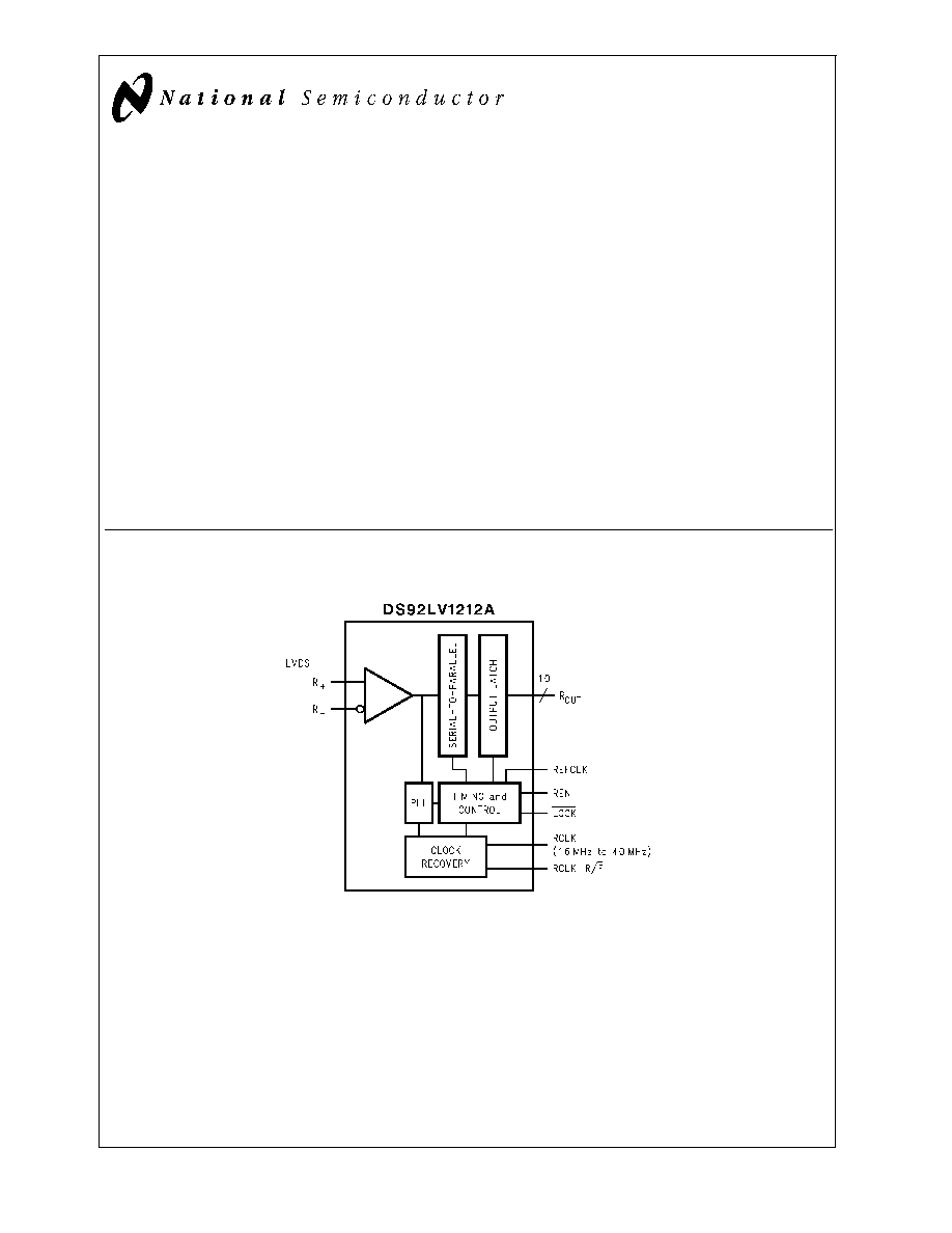
Block Diagram
TRI-STATE
�
is a registered trademark of National Semiconductor Corporation.
DS101387-1
November 2000
DS92L
V1212A
16-40
MHz
10-Bit
Bus
L
VDS
Random
Lock
Deserializer
with
Embedded
Clock
Recovery
� 2000 National Semiconductor Corporation
DS101387
www.national.com

Block Diagram
(Continued)
Functional Description
The DS92LV1212 is a 10-bit Deserializer chip designed to
receive data over heavily loaded differential backplanes at
clock speeds from 16 MHz to 40 MHz. It may also be used to
receive data over Unshielded Twisted Pair (UTP) cable.
The chip has three active states of operation: Initialization,
Data Transfer, and Resynchronization; and two passive
states: Powerdown and TRI-STATE
�
.
The following sections describe each operation of the active
and passive states.
Initialization
Before data can be transferred, the Deserializer must be
initialized. The Deserializer should be powered up with the
PWRDN pin held low. After V
CC
stabilizes, the PWRDN pin
can be forced high. The Deserializer is ready to lock to the
incoming data stream.
Step 1: When you apply V
CC
to the Deserializer, the respec-
tive outputs are held in TRI-STATE and internal circuitry is
disabled by on-chip power-on circuitry. When V
CC
reaches
V
CC
OK (2.5V), the PLL is ready to lock to incoming data or
synchronization patterns. You must apply the local clock to
the REFCLK pin.
The Deserializer LOCK output will remain high while its PLL
locks to incoming data or to SYNC patterns on the inputs.
Step 2: The Deserializer PLL must synchronize to the Seri-
alizer to complete the initialization. The Deserializer will lock
to non-repetitive data patterns; however, the transmission of
SYNC patterns to the Deserializer enables the Deserializer
to lock to the Serializer signal within a specified time. See
Figure 7.
The user's application determines control of the SYNC1 and
SYNC2 pins. One recommendation is a direct feedback loop
from the LOCK pin. Under all circumstances, the Serializer
stops sending SYNC patterns after both SYNC inputs return
low.
When the Deserializer detects edge transitions at the Bus
LVDS input, it will attempt to lock to the embedded clock
information. When the Deserializer locks to the Bus LVDS
clock, the LOCK output will go low. When LOCK is low, the
Deserializer outputs represent incoming Bus LVDS data.
Data Transfer
After initialization, the Serializer will accept data from inputs
DIN0�DIN9. The Serializer uses the TCLK input to latch
incoming Data. The TCLK_R/F pin selects which edge the
Serializer uses to strobe incoming data. TCLK_R/F high
selects the rising edge for clocking data and low selects the
falling edge. If either of the SYNC inputs is high for 5*TCLK
cycles, the data at DIN0-DIN9 is ignored regardless of clock
edge.
After determining which clock edge to use, a start and stop
bit, appended internally, frame the data bits in the register.
The start bit is always high and the stop bit is always low.
The start and stop bits function as the embedded clock bits
in the serial stream.
Serialized data and clock bits (10+2 bits) are received at 12
times the TCLK frequency. For example, if TCLK is 40 MHz,
the serial rate is 40 x 12 = 480 Mega bits per second. Since
only 10 bits are from input data, the serial "payload" rate is
10 times the TCLK frequency. For instance, if TCLK = 40
MHz, the payload data rate is 40 x 10 = 400 Mbps. TCLK is
provided by the data source and must be in the range 16
MHz to 40 MHz nominal.
The LOCK pin on the Deserializer is driven low when it is
synchronized with the Serializer. The Deserializer locks to
the embedded clock and uses it to recover the serialized
data. ROUT data is valid when LOCK is low. Otherwise,
ROUT0�ROUT9 is invalid.
The ROUT0-ROUT9 pins use the RCLK pin as the reference
to data. The polarity of the RCLK edge is controlled by the
RCLK_R/F input. See
Figure 5.
ROUT(0-9), LOCK and RCLK outputs will drive a minimum
of three CMOS input gates (15 pF load) with 40 MHz clock.
Resynchronization
When the Deserializer PLL locks to the embedded clock
edge, the Deserializer LOCK pin asserts a low. If the Dese-
rializer loses lock, the LOCK pin output will go high and the
outputs (including RCLK) will enter TRI-STATE.
The user's system monitors the LOCK pin to detect a loss of
synchronization. Upon detection, the system can arrange to
pulse the Serializer SYNC1 or SYNC2 pin to resynchronize.
Multiple resynchronization approaches are possible. One
Application
DS101387-2
DS92L
V1212A
www.national.com
2

Resynchronization
(Continued)
recommendation is to provide a feedback loop using the
LOCK pin itself to control the sync request of the Serializer
(SYNC1 or SYNC2). Dual SYNC pins are provided for mul-
tiple control in a multi-drop application. Sending sync pat-
terns for resynchronization is desirable when lock times
within a specific time are critical. However, the Deserializer
can lock to random data, which is discussed in the next
section.
Random Lock Initialization and
Resynchronization
The initialization and resynchronization methods described
in their respective sections are the fastest ways to establish
the link between the Serializer and Deserializer. However,
the DS92LV1212A can attain lock to a data stream without
requiring the Serializer to send special SYNC patterns. This
allows the DS92LV1212A to operate in "open-loop" applica-
tions. Equally important is the Deserializer's ability to support
hot insertion into a running backplane. In the open loop or
hot insertion case, we assume the data stream is essentially
random. Therefore, because lock time varies due to data
stream characteristics, we cannot possibly predict exact lock
time. The primary constraint on "random" lock time is the
initial phase relation between the incoming data and the
REFCLK when the Deserializer powers up. As described in
the next paragraph, the data contained in the data stream
can also affect lock time.
If a specific pattern is repetitive, the Deserializer could enter
"false lock" - falsely recognizing the data pattern as the
clocking bits. We refer to such a pattern as a repetitive
multi-transition, RMT. This occurs when more than one
Low-High transition takes place in a clock cycle over multiple
cycles. This occurs when any bit, except DIN 9, is held at a
low state and the adjacent bit is held high, creating a 0-1
transition. In the worst case, the Deserializer could become
locked to the data pattern rather than the clock. Circuitry
within the DS92LV1212A can detect that the possibility of
"false lock" exists. The circuitry accomplishes this by detect-
ing more than one potential position for clocking bits. Upon
detection, the circuitry will prevent the LOCK output from
becoming active until the potential "false lock" pattern
changes. The false lock detect circuitry expects the data will
eventually change, causing the Deserializer to lose lock to
the data pattern and then continue searching for clock bits in
the serial data stream. Graphical representations of RMT are
shown on the following page. Please note that RMT only
applies to bits DIN0-DIN8.
Powerdown
When no data transfer occurs, you can use the Powerdown
state. The Serializer and Deserializer use the Powerdown
state, a low power sleep mode, to reduce power consump-
tion. The Deserializer enters Powerdown when you drive
PWRDN and REN low. The Serializer enters Powerdown
when you drive PWRDN low. In Powerdown, the PLL stops
and the outputs enterTRI-STATE, which disables load cur-
rent and reduces supply current to the milliampere range. To
exit Powerdown, you must drive the PWRDN pin high.
Before valid data exchanges between the Serializer and
Deserializer, you must reinitialize and resynchronize the de-
vices to each other. Initialization of the Serializer takes 510
TCLK cycles. The Deserializer will initialize and assert LOCK
high until lock to the Bus LVDS clock occurs.
TRI-STATE
The Serializer enters TRI-STATE when the DEN pin is driven
low. This puts both driver output pins (DO+ and DO-) into
TRI-STATE. When you drive DEN high, the Serializer returns
to the previous state, as long as all other control pins remain
static (SYNC1, SYNC2, PWRDN, TCLK_R/F).
When you drive the REN pin low, the Deserializer enters
TRI-STATE.
Consequently,
the
receiver
output
pins
(ROUT0�ROUT9) and RCLK will enter TRI-STATE. The
LOCK output remains active, reflecting the state of the PLL.
DS92L
V1212A
www.national.com
3

RMT Patterns
Order Numbers
NSID
Function
Package
DS92LV1021TMSA
Serializer
MSA28
DS92LV1212AMSA
Deserializer
MSA28
DS101387-23
DIN0 Held Low-DIN1 Held High Creates an RMT Pattern
DS101387-24
DIN4 Held Low-DIN5 Held High Creates an RMT Pattern
DS101387-25
DIN8 Held Low-DIN9 Held High Creates an RMT Pattern
DS92L
V1212A
www.national.com
4

Absolute Maximum Ratings
(Note 1)
If Military/Aerospace specified devices are required,
please contact the National Semiconductor Sales Office/
Distributors for availability and specifications.
Supply Voltage (V
CC
)
-0.3V to +4V
CMOS/TTL Input Voltage
-0.3V to (V
CC
+0.3V)
CMOS/TTL Output Voltage
-0.3V to (V
CC
+0.3V)
Bus LVDS Receiver Input
Voltage
-0.3V to +3.9V
Junction Temperature
+150�C
Storage Temperature
-65�C to +150�C
Lead Temperature
(Soldering, 4 seconds)
+260�C
Maximum Package Power Dissipation Capacity
@
25�C Package:
28L SSOP
1.27 W
Package Derating:
28L SSOP
10.3mW/�C above +25�C
ESD Rating (HBM)
>
2kV
Recommended Operating
Conditions
Min
Nom
Max
Units
Supply Voltage (V
CC
)
3.0
3.3
3.6
V
Operating Free Air
Temperature (T
A
)
-40
+25
+85
�C
Receiver Input Range
0
2.4
V
Supply Noise Voltage
(V
CC
)
100 mV
P-P
Electrical Characteristics
Over recommended operating supply and temperature ranges unless otherwise specified.
Symbol
Parameter
Conditions
Min
Typ
Max
Units
DESERIALIZER LVCMOS/LVTTL DC SPECIFICATIONS (apply to pins PWRDN, RCLK_R/ F, REN, REFCLK = inputs; apply to
pins ROUT, RCLK, LOCK = outputs)
V
IH
High Level Input Voltage
2.0
V
CC
V
V
IL
Low Level Input Voltage
GND
0.8
V
V
CL
Input Clamp Voltage
I
CL
= -18 mA
-0.62
-1.5
V
I
IN
Input Current
V
IN
= 0V or 3.6V
-10
�
2
+15
�A
V
OH
High Level Output Voltage
I
OH
= -9 mA
2.1
2.93
V
CC
V
V
OL
Low Level Output Voltage
I
OL
= 9 mA
GND
0.33
0.5
V
I
OS
Output Short Circuit Current
VOUT = 0V
-15
-38
-85
mA
I
OZ
TRI-STATE Output Current
PWRDN or REN = 0.8V, V
OUT
= 0V or VCC
-10
�
0.4
+10
�A
DESERIALIZER Bus LVDS DC SPECIFICATIONS (apply to pins RI+ and RI-)
VTH
Differential Threshold High
Voltage
VCM = +1.1V
+6
+50
mV
VTL
Differential Threshold Low
Voltage
-50
-12
mV
I
IN
Input Current
V
IN
= +2.4V, V
CC
= 3.6V or 0V
-10
�
1
+15
�A
V
IN
= 0V, V
CC
= 3.6V or 0V
-10
�
0.05
+10
�A
DESERIALIZER SUPPLY CURRENT (apply to pins DVCC and AVCC)
I
CCR
Deserializer Supply Current
C
L
= 15 pF
f = 40 MHz
58
75
mA
Worst Case
Figure 1
f = 16 MHz
30
45
mA
I
CCXR
Deserializer Supply Current
Powerdown
PWRDN = 0.8V, REN = 0.8V
0.36
1.0
mA
Deserializer Timing Requirements for REFCLK
Over recommended operating supply and temperature ranges unless otherwise specified.
Symbol
Parameter
Conditions
Min
Typ
Max
Units
t
RFCP
REFCLK Period
25
T
62.5
ns
t
RFDC
REFCLK Duty Cycle
50
%
f
Ref
REFCLK Frequency
0.95/t
RCP
t
RCP
1.05/t
RCP
t
RFTT
REFCLK Transition Time
3
6
ns
DS92L
V1212A
www.national.com
5