 | –≠–ª–µ–∫—Ç—Ä–æ–Ω–Ω—ã–π –∫–æ–º–ø–æ–Ω–µ–Ω—Ç: DS96173CN | –°–∫–∞—á–∞—Ç—å:  PDF PDF  ZIP ZIP |

DS96173/DS96175
RS-485/RS-422 Quad Differential Line Receivers
General Description
The DS96173 and DS96175 are high speed quad differential
line receivers designed to meet EIA Standard RS-485. The
devices have TRI-STATE
Æ
outputs and are optimized for bal-
anced multipoint data bus transmission at rates up to 10
Mbps. The receivers feature high input impedance, input
hysteresis for increased noise immunity, and input sensitivity
of 200 mV over a common mode input voltage range of -7V
to +12V. The receivers are therefore suitable for multipoint
applications in noisy environments. The DS96173 features
an active high and active low Enable, common to all four re-
ceivers. The DS96175 features separate active high Enables
for each receiver pair. Compatible RS-485 drivers, transceiv-
ers, and repeaters are also offered to provide optimum bus
performance. The respective device types are DS96172,
DS96174, DS96176 and DS96177.
Features
n
Meets EIA Standard RS-485, RS-422A, RS-423A
n
Designed for multipoint bus applications
n
TRI-STATE Outputs
n
Common mode input voltage range: -7V to +12V
n
Operates from single +5V supply
n
Input sensitivity of
±
200 mV over common mode range
n
Input hysteresis of 50 mV typical
n
High input impedance
n
DS96173/DS96175 are lead and function compatible
with SN75173/75175 or the AM26LS32/MC3486
respectively
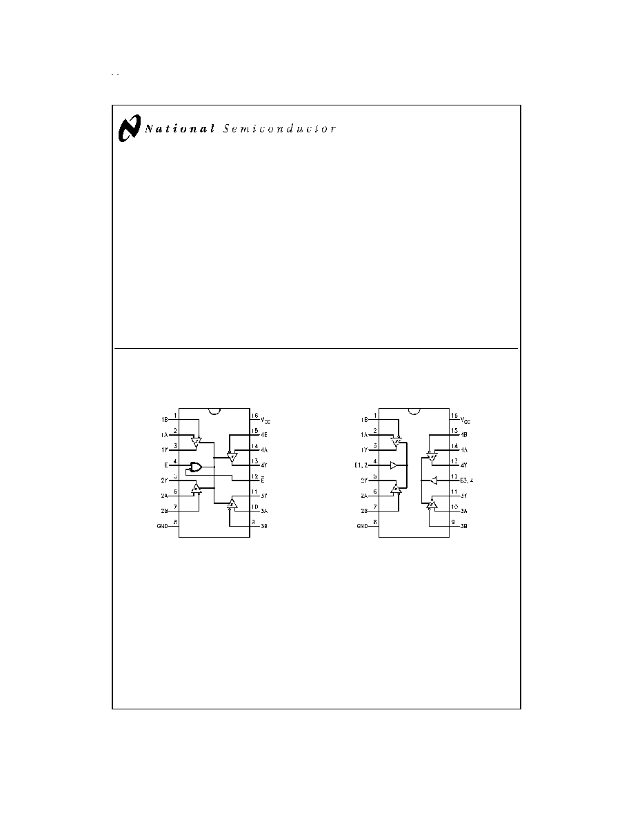
Connection Diagrams
TRI-STATE
Æ
is a registered trademark of National Semiconductor Corporation.
16-Lead DIP
DS96173
DS009628-1
16-Lead DIP
DS96175
DS009628-2
Order Number DS96173CN or DS96175CN
See NS Package Number N16E
June 1998
DS96173/DS96175
RS-485/RS-422
Quad
Differential
Line
Receivers
© 1998 National Semiconductor Corporation
DS009628
www.national.com

Absolute Maximum Ratings
(Note 2)
If Military/Aerospace specified devices are required,
please contact the National Semiconductor Sales Office/
Distributors for availability and specifications.
Storage Temperature Range
Molded DIP
-65∞C to +150∞C
Lead Temperature
Molded DIP (soldering, 10
sec.)
265∞C
Maximum Power Dissipation (Note 1) at 25∞C
N-Molded Package
1.84W
Supply Voltage
7V
Input Voltage, A or B Inputs
±
25V
Differential Input Voltage
±
25V
Enable Input Voltage
7V
Low Level Output Current
50 mA
Recommended Operating
Conditions
Min
Typ
Max
Units
Supply Voltage (V
CC
)
4.75
5
5.25
V
Common Mode Input
-7
+12
V
Voltage (V
CM
)
Differential Input
-7
+12
V
Voltage (V
ID
)
Output Current High (I
OH
)
-400
µA
Output Current LOW (I
OL
)
16
mA
Operating Temperature (T
A
)
0
25
70
∞C
Note 1: Derate molded DIP package 15 mW/∞C above 25∞C.
Electrical Characteristics
(Notes 3, 4)
over recommended temperature, common mode input voltage, and supply voltage ranges, unless otherwise specified
Symbol
Parameter
Conditions
Min
Typ
Max
Units
V
TH
Differential Input
V
O
= 2.7V, I
O
= - 0.4 mA
0.2
V
High Threshold Voltage
V
TL
Differential Input (Note 5)
V
O
= 0.5V, I
O
= 16 mA
-0.2
V
Low Threshold Voltage
V
T+
- V
T-
Hysteresis (Note 6)
V
CM
= 0V
50
mV
V
IH
Enable Input Voltage HIGH
2.0
V
V
IL
Enable Input Voltage LOW
0.8
V
V
IC
Enable Input Clamp Voltage
I
I
= -18 mA
-1.5
V
V
OH
Output Voltage HIGH
V
ID
= 200 mV, I
OH
= -400 µA
2.7
V
V
OL
Output Voltage LOW
V
ID
= -200 mV
I
OL
= 8 mA
0.45
V
I
OL
= 16 mA
0.50
I
OZ
High Impedance State Output
V
O
= 0.4V to 2.4V
±
20
µA
I
I
Line Input Current (Note 7)
Other Input = 0V
V
I
= 12V
1.0
mA
V
I
= -7V
-0.8
I
IH
Enable Input Current HIGH
V
IH
= 2.7V
20
µA
I
IL
Enable Input Current LOW
V
IL
= 0.4V
-100
µA
R
I
Input Resistance
12
k
I
OS
Short Circuit Output Current
(Note 8)
-15
-85
mA
I
CC
Supply Current
Outputs Disabled
75
mA
Note 2: "Absolute Maximum Ratings" are those values beyond which the safety of the device cannot be guaranteed. They are not meant to imply that the devices
should be operated at these limits. The tables of "Electrical Characteristics" provide conditions for actual device operation.
Note 3: Unless otherwise specified Min/Max limits apply across the 0∞C to +70∞C range for the DS96173/DS96175. All typicals are given for V
CC
= 5V and T
A
= 25∞C.
Note 4: All currents into the device pins are positive; all currents out of the device pins are negative. All voltages are reference to ground unless otherwise specified.
Note 5: The algebraic convention, when the less positive (more negative) limit is designated minimum, is used in this data sheet for common mode input voltage
and threshold voltage levels only.
Note 6: Hysteresis is the difference between the positive-going input threshold voltage, V
T+
, and the negative going input threshold voltage, V
T-
.
Note 7: Refer to EIA Standards RS-485 for exact conditions.
Note 8: Only one output at a time should be shorted.
www.national.com
2

Switching Characteristics
V
CC
= 5V, T
A
= 25∞C
Symbol
Parameter
Conditions
Min
Typ
Max
Units
t
PLH
Propagation Delay Time,
V
ID
= -2.5V to 2.5V,
15
25
ns
Low to High Level Output
C
L
= 15 pF,
Figure 1
t
PHL
Propagation Delay Time,
15
25
ns
High to Low Level Output
t
PZH
Output Enable Time to High Level
C
L
= 15 pF,
Figure 2
15
22
ns
t
PZL
Output Enable Time to Low Level
C
L
= 15 pF,
Figure 3
15
22
ns
t
PHZ
Output Disable Time from High Level
C
L
= 5 pF,
Figure 2
14
30
ns
t
PLZ
Output Disable Time from Low Level
C
L
= 5 pF,
Figure 3
24
40
ns
Function Tables
(Each Receiver) DS96173
Differential Inputs
Enables
Outputs
A≠B
E
E
V
V
ID
>
0.2V
H
X
H
X
L
H
V
ID
<
-0.2V
H
X
L
X
L
L
X
L
X
Z
X
X
H
Z
H = High Level
L = Low Level
X = Immaterial
Z = High Impedance (off)
(Each Receiver) DS96175
Differential Inputs
Enable
Output
A≠B
Y
V
ID
0.2V
H
H
V
ID
-0.2V
H
L
X
L
Z
Parameter Measurement Information
DS009628-3
DS009628-4
FIGURE 1. t
PLH
, t
PHL
(Note 11)
www.national.com
3

Parameter Measurement Information
(Continued)
Note 9: The input pulse is supplied by a generator having the following characteristics: PRR = 1.0 MHz, 50% duty cycle, t
r
6.0 ns, t
f
6.0 ns, Z
O
= 50
.
Note 10: C
L
includes probe and stray capacitance.
Note 11: DS96173 with active high and active low Enables is shown here. DS96175 has active high Enable only.
Note 12: All diodes are 1N916 or equivalent.
Note 13: To test the active low Enable E of DS96173, ground E and apply an inverted input waveform to E . DS96175 has active high Enable only.
Typical Application
DS009628-5
DS009628-6
FIGURE 2. t
PHZ
, t
PZH
(Note 11)
DS009628-7
DS009628-8
FIGURE 3. t
PZL
, t
PLZ
(Note 11)
DS009628-9
Note: The line length should be terminated at both ends in its characteristic impedance. Stub lengths off the main line should be kept as short as possible.
FIGURE 4.
www.national.com
4

5


