 | ÐлекÑÑоннÑй компоненÑ: DS96176CN | СкаÑаÑÑ:  PDF PDF  ZIP ZIP |
Äîêóìåíòàöèÿ è îïèñàíèÿ www.docs.chipfind.ru
DS96176
RS-485/RS-422 Differential Bus Transceiver
General Description
The DS96176 Differential Bus Transceiver is a monolithic in-
tegrated circuit designed for bidirectional data communica-
tion on balanced multipoint bus transmission lines. The
transceiver meets EIA Standard RS-485 as well as
RS-422A.
The DS96176 combines a TRI-STATE
®
differential line driver
and a differential input line receiver, both of which operate
from a single 5.0V power supply. The driver and receiver
have an active Enable that can be externally connected to
function as a direction control. The driver differential outputs
and the receiver differential inputs are internally connected
to form differential input/output (I/O) bus ports that are de-
signed to offer minimum loading to the bus whenever the
driver is disabled or when V
CC
= 0V. These ports feature
wide positive and negative common mode voltage ranges,
making the device suitable for multipoint applications in
noisy environments.
The driver is designed to handle loads up to 60 mA of sink or
source current. The driver features positive and negative
current-limiting and thermal shutdown for protection from line
fault conditions. Thermal shutdown is designed to occur at
junction temperature of approximately 160°C. The receiver
features a typical input impedance of 15 k
, an input sensi-
tivity of
±
200 mV, and a typical input hysteresis of 50 mV.
The DS96176 can be used in transmission line applications
employing the DS96172 and the DS96174 quad differential
line drivers and the DS96173 and DS96175 quad differential
line receivers.
Features
n
Bidirectional transceiver
n
Meets EIA Standard RS-422A and RS-485
n
Designed for multipoint transmission
n
TRI-STATE driver and receiver enables
n
Individual driver and receiver enables
n
Wide positive and negative input/output bus voltage
ranges
n
Driver output capability
±
60 mA Maximum
n
Thermal shutdown protection
n
Driver positive and Negative current-limiting
n
High impedance receiver input
n
Receiver input sensitivity of
±
200 mV
n
Receiver input hysteresis of 50 mV typical
n
Operates from single 5.0V supply
n
Low power requirements
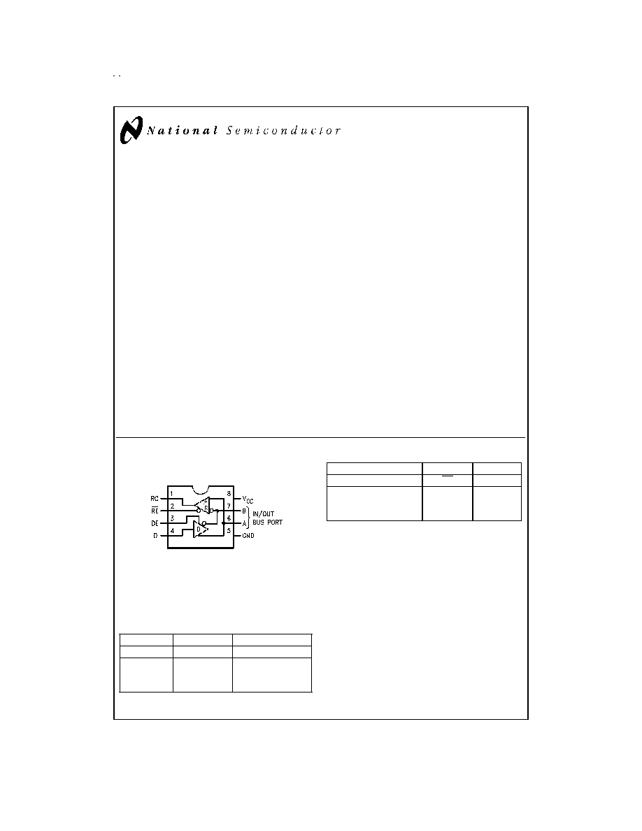
Connection Diagram
Function Table
Driver
Input
Enable
Outputs
DI
DE
A
B
H
H
H
L
L
H
L
H
X
L
Z
Z
Receiver
Differential Inputs
Enable
Output
A-B
RE
R
V
ID
0.2V
L
H
V
ID
-0.2V
L
L
X
H
Z
H = High Level
L = Low Level
X = Immaterial
Z = High Impedance (off)
TRI-STATE
®
is a registered trademark of National Semiconductor Corporation.
8Lead DIP
DS009630-1
Top View
Order Number DS96176CN
See NS Package Number N08E
May 1998
DS96176
RS-485/RS-422
Differential
Bus
T
ransceiver
© 1998 National Semiconductor Corporation
DS009630
www.national.com
Absolute Maximum Ratings
(Note 2)
If Military/Aerospace specified devices are required,
please contact the National Semiconductor Sales Office/
Distributors for availability and specifications.
Storage Temperature Range
Molded DIP
-65°C to +150°C
Lead Temperature
Molded DIP (soldering, 10
sec.)
265°C
Maximum Power Dissipation (Note 1) at 25°C
Molded Package
930 mW
Supply Voltage
7.0V
Differential Input Voltage
+15V/-10V
Enable Input Voltage
5.5V
Recommended Operating
Conditions
Min
Typ
Max
Units
Supply Voltage (V
CC
)
4.75
5.0
5.25
V
Voltage at Any Bus Terminal
(Separately or Common Mode)
-7.0
12
V
Differential Input Voltage (V
ID
)
±
12
V
Output Current HIGH (I
OH
)
Driver
-60
mA
Receiver
-400
µA
Output Current LOW (I
OL
)
Driver
60
mA
Receiver
16
mA
Operating Temperature (T
A
)
0
25
70
°C
Note 1: Derate molded DIP package 7.5 mW/°C above 25°C.
Electrical Characteristics
(Notes 3, 4)
Over recommended temperature, common mode input voltage, and supply voltage ranges, unless otherwise specified
Symbol
Parameter
Conditions
Min
Typ
Max
Units
DRIVER SECTION
V
IH
Input Voltage HIGH
2.0
V
V
IL
Input Voltage LOW
0.8
V
V
OH
Output Voltage HIGH
I
OH
= -20 mA
3.1
V
V
OL
Output Voltage LOW
I
OL
= 20 mA
0.85
V
V
IC
Input Clamp Voltage
I
I
= -18 mA
-1.5
V
|V
OD1
|
Differential Output Voltage
I
O
= 0 mA
6.0
V
|V
OD2
|
Differential Output Voltage
R
L
= 100
,
Figure 1
2.0
2.25
V
R
L
= 54
,
Figure 1 and Figure 2
1.5
2.0
|V
OD2
|
Change in Magnitude of
R
L
= 54
Differential Output Voltage (Note 5)
V
CM
= 0V Figure 1 and Figure 2
±
0.2
V
R
L
= 100
Figure 1
V
OC
Common Mode Output Voltage (Note 6)
R
L
= 54
or 100
,
Figure 1
3.0
V
|V
OC
|
Change in Magnitude of
±
0.2
V
Common Mode Output Voltage (Note 5)
I
O
Output Current (Note 5)
Output Disabled
V
O
= 12V
1.0
mA
(Includes Receiver I
I
)
V
O
= -7.0V
-0.8
I
IH
Input Current HIGH
V
I
= 2.4V
20
µA
I
IL
Input Current LOW
V
I
= 0.4V
-100
µA
I
OS
Short Circuit Output Current
V
O
= -7.0V
-250
(Note 10)
V
O
= 0V
-150
mA
V
O
= V
CC
150
V
O
= 12V
250
I
CC
Supply Current
No Load
Outputs Enabled
35
mA
Outputs Disabled
40
RECEIVER SECTION
V
TH
Differential Input High
V
O
= 2.7V, I
O
= -0.4 mA
0.2
V
Threshold Voltage
V
TL
Differential Input Low
V
O
= 0.5V, I
O
= 8.0 mA
-0.2
V
Threshold Voltage (Note 7)
V
T+
- V
T-
Hysteresis (Note 8)
V
CM
= 0V
50
mV
V
IH
Enable Input Voltage HIGH
2.0
V
V
IL
Enable Input Voltage LOW
0.8
V
V
IC
Enable Input Clamp Voltage
I
I
= -18 mA
-1.5
V
www.national.com
2
Electrical Characteristics
(Notes 3, 4) (Continued)
Over recommended temperature, common mode input voltage, and supply voltage ranges, unless otherwise specified
Symbol
Parameter
Conditions
Min
Typ
Max
Units
RECEIVER SECTION
V
OH
Output Voltage HIGH
V
ID
= 200 mV, I
OH
= -400 µA,
2.7
V
Figure 3
V
OL
Output Voltage LOW
V
ID
= -200 mV,
I
OL
= 8,0 mA
0.45
V
Figure 3
I
OL
= 16 mA
0.50
I
OZ
High Impedance State Output
V
O
= 0.45V to 2.4V
±
20
µA
I
I
Line Input Current (Note 9)
Other Input =
0V
V
I
= 12V
1.0
mA
V
I
= -7.0V
0.8
I
IH
Enable Input Current HIGH
V
IH
= 2.7V
20
µA
I
IL
Enable Input Current LOW
V
IL
= 0.4V
-100
µA
R
I
Input Resistance
12
k
I
OS
Short Circuit Output Current
(Note 10)
-15
-85
mA
I
CC
Supply Current (Total Package)
No Load
Outputs Enabled
40
mA
Outputs Disabled
Driver Switching Characteristics
V
CC
= 5V, T
A
= 25°C
Symbol
Parameter
Conditions
Min
Typ
Max
Units
t
DD
Differential Output Delay Time
R
L
= 60
,
Figure 4
15
25
ns
t
TD
Differential Output Transition Time
R
L
= 60
,
Figure 4
15
25
ns
t
PLH
Propagation Delay Time,
R
L
= 27
,
Figure 5
12
20
ns
Low-to-High Level Output
t
PHL
Propagation Delay Time,
R
L
= 27
,
Figure 5
12
20
ns
High-to-Low Level Output
t
PZH
Output Enable Time to High Level
R
L
= 110
,
Figure 6
25
35
ns
t
PZL
Output Enable Time to Low Level
R
L
= 110
,
Figure 7
25
35
ns
t
PHZ
Output Disable Time from High Level
R
L
= 110
,
Figure 6
20
25
ns
t
PLZ
Output Disable Time from Low Level
R
L
= 110
,
Figure 7
29
35
ns
Receiver Switching Characteristics
V
CC
= 5.0V, T
A
= 25°C
Symbol
Parameter
Conditions
Min
Typ
Max
Units
t
PLH
Propagation Delay Time,
V
ID
= 0V to 3.0V
16
25
ns
Low-to-High Level Output
C
L
= 15 pF, Figure 8
t
PHL
Propagation Delay Time,
16
25
ns
High-to-Low Level Output
t
PZH
Output Enable Time to High Level
C
L
= 15 pF, Figure 9
15
22
ns
t
PZL
Output Enable Time to Low Level
15
22
ns
t
PHZ
Output Disable Time from High Level
C
L
= 5.0 pF, Figure 9
14
30
ns
t
PLZ
Output Disable Time from Low Level
24
40
ns
Note 2: "Absolute Maximum Ratings" are those values beyond which the safety of the device cannot be guaranteed. They are not meant to imply that the devices
should be operated at these limits. The tables of "Electrical Characteristics" provide conditions for actual operation.
Note 3: Unless otherwise specified min/max limits apply across the 0°C to +70°C range for the DS96176. All typicals are given for V
CC
= 5V and T
A
= 25°C.
Note 4: All currents into the device pins are positive; all currents out of the device pins are negative. All voltages are referenced to ground unless otherwise specified.
Note 5:
|V
OD
| and
|V
OC
| are the changes in magnitude of V
OD
and V
OC
, respectively, that occur when the input is changed from a high level to a low level.
Note 6: In EIA Standards RS-422A and RS-485, V
OC
, which is the average of the two output voltages with respect to ground, is called output offset voltage, V
OS
.
Note 7: The algebraic convention, where the less positive (more negative) limit is designated minimum, is used in this data sheet for common mode input voltage
and threshold voltage levels only.
Note 8: Hysteresis is the difference between the positive-going input threshold voltage V
T+
, and the negative-going input threshold voltage, V
T-
.
www.national.com
3
Receiver Switching Characteristics
(Continued)
Note 9: Refer to EIA Standard RS-485 for exact conditions.
Note 10: Only one output at a time should be shorted.
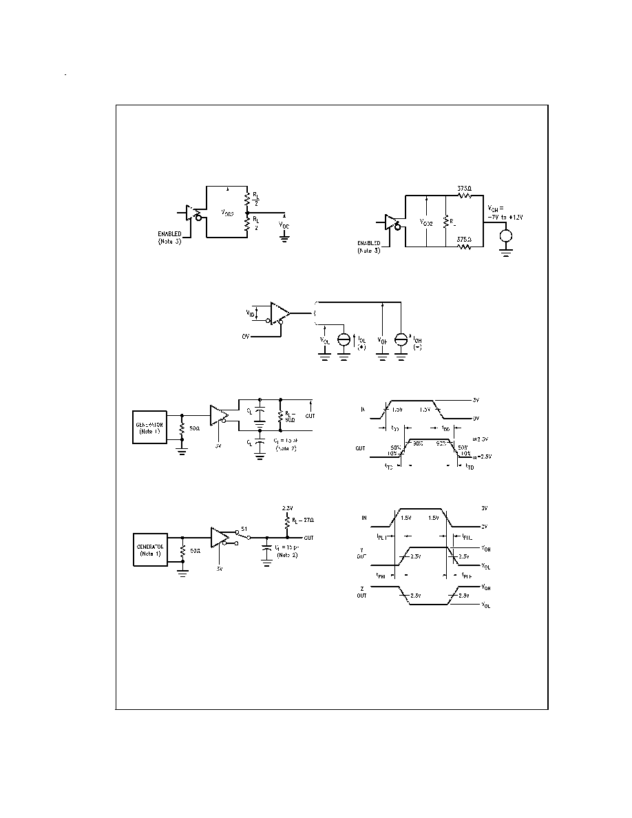
Parameter Measurement Information
DS009630-2
FIGURE 1. Driver V
OD
and V
OC
DS009630-3
FIGURE 2. Driver V
OD
with Varying
Common Mode Voltage
DS009630-4
FIGURE 3. Receiver V
OH
and V
OL
DS009630-5
DS009630-6
FIGURE 4. Driver Differential Output Delay and Transition Times
DS009630-7
DS009630-8
FIGURE 5. Driver Propagation Times
www.national.com
4
Parameter Measurement Information
(Continued)
DS009630-9
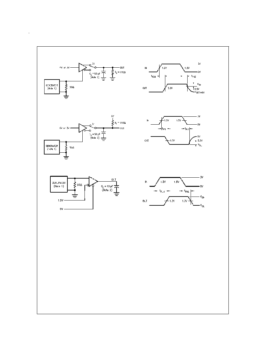
DS009630-10
FIGURE 6. Driver Enable and Disable Times (t
PZH
, t
PHZ
)
DS009630-11
DS009630-12
FIGURE 7. Driver Enable and Disable Times (t
PZL
, t
PLZ
)
DS009630-13
DS009630-14
FIGURE 8. Receiver Propagation Delay Times
www.national.com
5