LM118/LM218/LM318
Operational Amplifiers
General Description
The LM118 series are precision high speed operational am-
plifiers designed for applications requiring wide bandwidth
and high slew rate. They feature a factor of ten increase in
speed over general purpose devices without sacrificing DC
performance.
The LM118 series has internal unity gain frequency compen-
sation. This considerably simplifies its application since no
external components are necessary for operation. However,
unlike most internally compensated amplifiers, external fre-
quency compensation may be added for optimum perfor-
mance. For inverting applications, feedforward compensa-
tion will boost the slew rate to over 150V/µs and almost
double the bandwidth. Overcompensation can be used with
the amplifier for greater stability when maximum bandwidth
is not needed. Further, a single capacitor can be added to re-
duce the 0.1% settling time to under 1 µs.
The high speed and fast settling time of these op amps make
them useful in A/D converters, oscillators, active filters,
sample and hold circuits, or general purpose amplifiers.
These devices are easy to apply and offer an order of mag-
nitude better AC performance than industry standards such
as the LM709.
The LM218 is identical to the LM118 except that the LM218
has its performance specified over a -25∞C to +85∞C tem-
perature range. The LM318 is specified from 0∞C to +70∞C.
Features
n
15 MHz small signal bandwidth
n
Guaranteed 50V/µs slew rate
n
Maximum bias current of 250 nA
n
Operates from supplies of
±
5V to
±
20V
n
Internal frequency compensation
n
Input and output overload protected
n
Pin compatible with general purpose op amps
Fast Voltage Follower
(Note 1)
DS007766-13
Note 1: Do not hard-wire as voltage follower (R1
5 k
)
August 2000
LM1
18/LM218/LM318
Operational
Amplifiers
© 2000 National Semiconductor Corporation
DS007766
www.national.com

Absolute Maximum Ratings
(Note 7)
If Military/Aerospace specified devices are required,
please contact the National Semiconductor Sales Office/
Distributors for availability and specifications.
Supply Voltage
±
20V
Power Dissipation (Note 2)
500 mW
Differential Input Current (Note 3)
±
10 mA
Input Voltage (Note 4)
±
15V
Output Short-Circuit Duration
Continuous
Operating Temperature Range
LM118
-55∞C to +125∞C
LM218
-25∞C to +85∞C
LM318
0∞C to +70∞C
Storage Temperature Range
-65∞C to +150∞C
Lead Temperature (Soldering, 10 sec.)
Hermetic Package
300∞C
Plastic Package
260∞C
Soldering Information
Dual-In-Line Package
Soldering (10 sec.)
260∞C
Small Outline Package
Vapor Phase (60 sec.)
215∞C
Infrared (15 sec.)
220∞C
See AN-450 "Surface Mounting Methods and Their Effect
on Product Reliability" for other methods of soldering
surface mount devices.
ESD Tolerance (Note 8)
2000V
Electrical Characteristics
(Note 5)
Parameter
Conditions
LM118/LM218
LM318
Units
Min
Typ
Max
Min
Typ
Max
Input Offset Voltage
T
A
= 25∞C
2
4
4
10
mV
Input Offset Current
T
A
= 25∞C
6
50
30
200
nA
Input Bias Current
T
A
= 25∞C
120
250
150
500
nA
Input Resistance
T
A
= 25∞C
1
3
0.5
3
M
Supply Current
T
A
= 25∞C
5
8
5
10
mA
Large Signal Voltage Gain
T
A
= 25∞C, V
S
=
±
15V
50
200
25
200
V/mV
V
OUT
=
±
10V, R
L
2 k
Slew Rate
T
A
= 25∞C, V
S
=
±
15V, A
V
= 1
50
70
50
70
V/µs
(Note 6)
Small Signal Bandwidth
T
A
= 25∞C, V
S
=
±
15V
15
15
MHz
Input Offset Voltage
6
15
mV
Input Offset Current
100
300
nA
Input Bias Current
500
750
nA
Supply Current
T
A
= 125∞C
4.5
7
mA
Large Signal Voltage Gain
V
S
=
±
15V, V
OUT
=
±
10V
25
20
V/mV
R
L
2 k
Output Voltage Swing
V
S
=
±
15V, R
L
= 2 k
±
12
±
13
±
12
±
13
V
Input Voltage Range
V
S
=
±
15V
±
11.5
±
11.5
V
Common-Mode Rejection Ratio
80
100
70
100
dB
Supply Voltage Rejection Ratio
70
80
65
80
dB
Note 2: The maximum junction temperature of the LM118 is 150∞C, the LM218 is 110∞C, and the LM318 is 110∞C. For operating at elevated temperatures, devices
in the H08 package must be derated based on a thermal resistance of 160∞C/W, junction to ambient, or 20∞C/W, junction to case. The thermal resistance of the
dual-in-line package is 100∞C/W, junction to ambient.
Note 3: The inputs are shunted with back-to-back diodes for overvoltage protection. Therefore, excessive current will flow if a differential input voltage in excess of
1V is applied between the inputs unless some limiting resistance is used.
Note 4: For supply voltages less than
±
15V, the absolute maximum input voltage is equal to the supply voltage.
Note 5: These specifications apply for
±
5V
V
S
±
20V and -55∞C
T
A
+125∞C (LM118), -25∞C
T
A
+85∞C (LM218), and 0∞C
T
A
+70∞C (LM318). Also,
power supplies must be bypassed with 0.1 µF disc capacitors.
Note 6: Slew rate is tested with V
S
=
±
15V. The LM118 is in a unity-gain non-inverting configuration. V
IN
is stepped from -7.5V to +7.5V and vice versa. The slew
rates between -5.0V and +5.0V and vice versa are tested and guaranteed to exceed 50V/µs.
Note 7: Refer to RETS118X for LM118H and LM118J military specifications.
Note 8: Human body model, 1.5 k
in series with 100 pF.
LM1
18/LM218/LM318
www.national.com
2

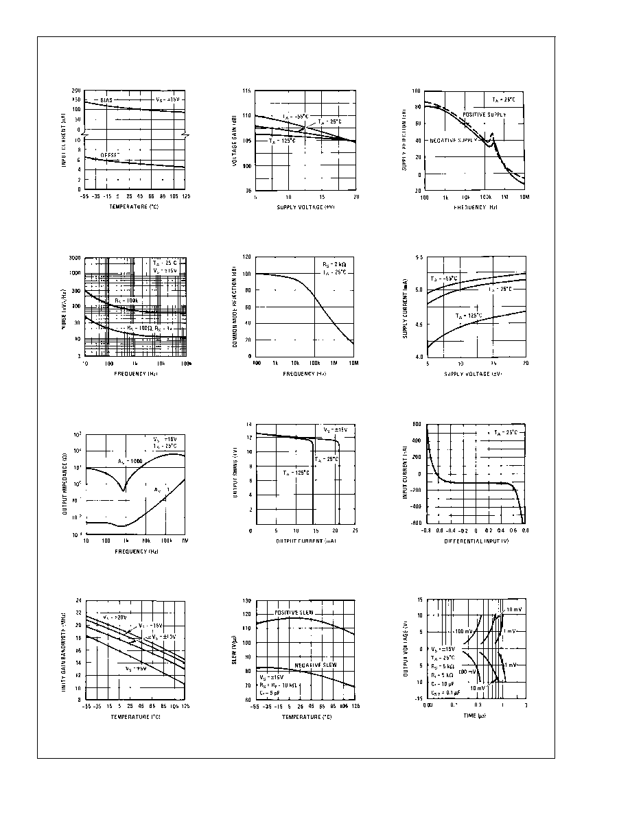
Typical Performance Characteristics
LM118, LM218 (Continued)
Typical Performance Characteristics
LM318
Large Signal Frequency
Response
DS007766-37
Open Loop Frequency
Response
DS007766-38
Voltage Follower Pulse
Response
DS007766-39
Large Signal Frequency
Response
DS007766-40
Open Loop Frequency
Response
DS007766-41
Inverter Pulse Response
DS007766-42
Input Current
DS007766-43
Voltage Gain
DS007766-44
Power Supply Rejection
DS007766-45
LM1
18/LM218/LM318
www.national.com
4