 | –≠–ª–µ–∫—Ç—Ä–æ–Ω–Ω—ã–π –∫–æ–º–ø–æ–Ω–µ–Ω—Ç: LF351 | –°–∫–∞—á–∞—Ç—å:  PDF PDF  ZIP ZIP |
TL H 5648
LF351
Wide
Bandwidth
JFET
Input
Operational
Amplifier
December 1995
LF351 Wide Bandwidth JFET Input Operational Amplifier
General Description
The LF351 is a low cost high speed JFET input operational
amplifier with an internally trimmed input offset voltage
(BI-FET II
TM
technology) The device requires a low supply
current and yet maintains a large gain bandwidth product
and a fast slew rate In addition well matched high voltage
JFET input devices provide very low input bias and offset
currents The LF351 is pin compatible with the standard
LM741 and uses the same offset voltage adjustment circuit-
ry This feature allows designers to immediately upgrade the
overall performance of existing LM741 designs
The LF351 may be used in applications such as high speed
integrators fast D A converters sample-and-hold circuits
and many other circuits requiring low input offset voltage
low input bias current high input impedance high slew rate
and wide bandwidth The device has low noise and offset
voltage drift but for applications where these requirements
are critical the LF356 is recommended If maximum supply
current is important however the LF351 is the better
choice
Features
Y
Internally trimmed offset voltage
10 mV
Y
Low input bias current
50 pA
Y
Low input noise voltage
25 nV
0
Hz
Y
Low input noise current
0 01 pA
0
Hz
Y
Wide gain bandwidth
4 MHz
Y
High slew rate
13 V ms
Y
Low supply current
1 8 mA
Y
High input impedance
10
12
X
Y
Low total harmonic distortion A
V
e
10
k
0 02%
R
L
e
10k V
O
e
20 Vp-p BW
e
20 Hz ≠ 20 kHz
Y
Low 1 f noise corner
50 Hz
Y
Fast settling time to 0 01%
2 ms
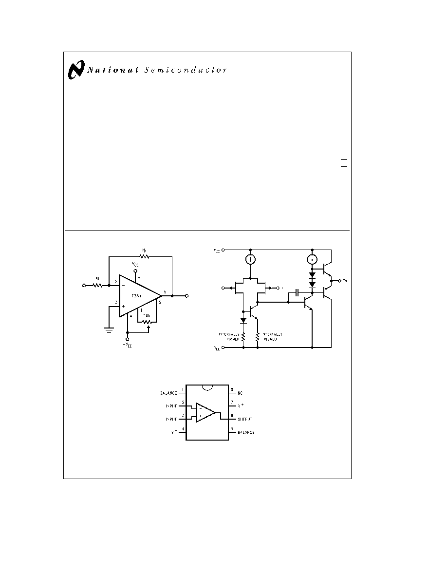
Typical Connection
TL H 5648 ≠ 11
Simplified Schematic
TL H 5648 ≠ 12
Connection Diagrams
Dual-In-Line Package
TL H 5648 ≠ 13
Order Number LF351M or LF351N
See NS Package Number M08A or N08E
C1995 National Semiconductor Corporation
RRD-B30M125 Printed in U S A
Absolute Maximum Ratings
If Military Aerospace specified devices are required
please contact the National Semiconductor Sales
Office Distributors for availability and specifications
Supply Voltage
g
18V
Power Dissipation (Notes 1 and 6)
670 mW
Operating Temperature Range
0 C to
a
70 C
T
j(MAX)
115 C
Differential Input Voltage
g
30V
Input Voltage Range (Note 2)
g
15V
Output Short Circuit Duration
Continuous
Storage Temperature Range
b
65 C to
a
150 C
Lead Temp (Soldering 10 sec )
Metal Can
300 C
DIP
260 C
i
jA
N Package
120 C W
M Package
TBD
Soldering Information
Dual-In-Line Package
Soldering (10 sec )
260 C
Small Outline Package
Vapor Phase (60 sec )
215 C
Infrared (15 sec )
220 C
See AN-450 ``Surface Mounting Methods and Their Effect
on Product Reliability'' for other methods of soldering sur-
face mount devices
ESD rating to be determined
DC Electrical Characteristics
(Note 3)
Symbol
Parameter
Conditions
LF351
Units
Min
Typ
Max
V
OS
Input Offset Voltage
R
S
e
10 kX T
A
e
25 C
5
10
mV
Over Temperature
13
mV
D
V
OS
D
T
Average TC of Input Offset
R
S
e
10 kX
10
m
V C
Voltage
I
OS
Input Offset Current
T
j
e
25 C (Notes 3 4)
25
100
pA
T
j
s
70 C
4
nA
I
B
Input Bias Current
T
j
e
25 C (Notes 3 4)
50
200
pA
T
j
s g
70 C
8
nA
R
IN
Input Resistance
T
j
e
25 C
10
12
X
A
VOL
Large Signal Voltage Gain
V
S
e
g
15V T
A
e
25 C
25
100
V mV
V
O
e
g
10V R
L
e
2 kX
Over Temperature
15
V mV
V
O
Output Voltage Swing
V
S
e
g
15V R
L
e
10 kX
g
12
g
13 5
V
V
CM
Input Common-Mode Voltage
a
15
V
Range
V
S
e
g
15V
g
11
b
12
V
CMRR
Common-Mode Rejection Ratio
R
S
s
10 kX
70
100
dB
PSRR
Supply Voltage Rejection Ratio
(Note 5)
70
100
dB
I
S
Supply Current
1 8
3 4
mA
2

AC Electrical Characteristics
(Note 3)
Symbol
Parameter
Conditions
LF351
Units
Min
Typ
Max
SR
Slew Rate
V
S
e
g
15V T
A
e
25 C
13
V ms
GBW
Gain Bandwidth Product
V
S
e
g
15V T
A
e
25 C
4
MHz
e
n
Equivalent Input Noise Voltage
T
A
e
25 C R
S
e
100X
25
nV
0
Hz
f
e
1000 Hz
i
n
Equivalent Input Noise Current
T
j
e
25 C f
e
1000 Hz
0 01
pA
0
Hz
Note 1
For operating at elevated temperature the device must be derated based on the thermal resistance i
JA
Note 2
Unless otherwise specified the absolute maximum negative input voltage is equal to the negative power supply voltage
Note 3
These specifications apply for V
S
e g
15V and 0 C
s
T
A
s a
70 C V
OS
I
B
and I
OS
are measured at V
CM
e
0
Note 4
The input bias currents are junction leakage currents which approximately double for every 10 C increase in the junction temperature T
j
Due to the limited
production test time the input bias currents measured are correlated to junction temperature In normal operation the junction temperature rises above the ambient
temperature as a result of internal power dissipation P
D
T
j
e
T
A
a
i
jA
P
D
where i
jA
is the thermal resistance from junction to ambient Use of a heat sink is
recommended if input bias current is to be kept to a minimum
Note 5
Supply voltage rejection ratio is measured for both supply magnitudes increasing or decreasing simultaneously in accordance with common practice From
g
15V to
g
5V
Note 6
Max Power Dissipation is defined by the package characteristics Operating the part near the Max Power Dissipation may cause the part to operate
outside guaranteed limits
3

Typical Performance Characteristics
Input Bias Current
Input Bias Current
Supply Current
Positive Common-Mode
Input Voltage Limit
Negative Common-Mode
Input Voltage Limit
Positive Current Limit
Negative Current Limit
Voltage Swing
Output Voltage Swing
Gain Bandwidth
Bode Plot
Slew Rate
TL H 5648 ≠ 2
4

Typical Performance Characteristics
(Continued)
Distortion vs Frequency
Undistorted Output
Voltage Swing
Open Loop Frequency
Response
Common-Mode
Rejection Ratio
Power Supply
Rejection Ratio
Equivalent Input
Noise Voltage
Open Loop Voltage
Gain (V V)
Output Impedance
Inverter Settling Time
TL H 5648 ≠ 3
5