LF353
Wide Bandwidth Dual JFET Input Operational Amplifier
General Description
These devices are low cost, high speed, dual JFET input
operational amplifiers with an internally trimmed input offset
voltage (BI-FET II
TM
technology). They require low supply
current yet maintain a large gain bandwidth product and fast
slew rate. In addition, well matched high voltage JFET input
devices provide very low input bias and offset currents. The
LF353 is pin compatible with the standard LM1558 allowing
designers to immediately upgrade the overall performance of
existing LM1558 and LM358 designs.
These amplifiers may be used in applications such as high
speed integrators, fast D/A converters, sample and hold
circuits and many other circuits requiring low input offset
voltage, low input bias current, high input impedance, high
slew rate and wide bandwidth. The devices also exhibit low
noise and offset voltage drift.
Features
n
Internally trimmed offset voltage:
10 mV
n
Low input bias current:
50pA
n
Low input noise voltage:
25 nV/
Hz
n
Low input noise current:
0.01 pA/
Hz
n
Wide gain bandwidth:
4 MHz
n
High slew rate:
13 V/�s
n
Low supply current:
3.6 mA
n
High input impedance:
10
12
n
Low total harmonic distortion :
0.02%
n
Low 1/f noise corner:
50 Hz
n
Fast settling time to 0.01%:
2 �s
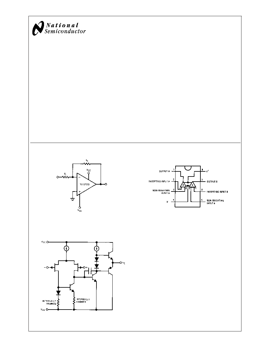
Typical Connection
00564914
Simplified Schematic
1/2 Dual
00564916
Connection Diagram
Dual-In-Line Package
00564917
Top View
Order Number LF353M, LF353MX or LF353N
See NS Package Number M08A or N08E
BI-FET II
TM
is a trademark of National Semiconductor Corporation.
December 2003
LF353
W
ide
Bandwidth
Dual
JFET
Input
Operational
Amplifier
� 2003 National Semiconductor Corporation
DS005649
www.national.com
Absolute Maximum Ratings
(Note 1)
If Military/Aerospace specified devices are required,
please contact the National Semiconductor Sales Office/
Distributors for availability and specifications.
Supply Voltage
�
18V
Power Dissipation
(Note 2)
Operating Temperature Range
0�C to +70�C
T
j
(MAX)
150�C
Differential Input Voltage
�
30V
Input Voltage Range (Note 3)
�
15V
Output Short Circuit Duration
Continuous
Storage Temperature Range
-65�C to +150�C
Lead Temp. (Soldering, 10 sec.)
260�C
Soldering Information
Dual-In-Line Package
Soldering (10 sec.)
260�C
Small Outline Package
Vapor Phase (60 sec.)
215�C
Infrared (15 sec.)
220�C
See AN-450 "Surface Mounting Methods and Their Effect
on Product Reliability" for other methods of soldering
surface mount devices.
ESD Tolerance (Note 8)
1000V
JA
M Package
TBD
Note 1: Absolute Maximum Ratings indicate limits beyond which damage to
the device may occur. Operating ratings indicate conditions for which the
device is functional, but do not guarantee specific performance limits. Elec-
trical Characteristics state DC and AC electrical specifications under particu-
lar test conditions which guarantee specific performance limits. This assumes
that the device is within the Operating Ratings. Specifications are not guar-
anteed for parameters where no limit is given, however, the typical value is a
good indication of device performance.
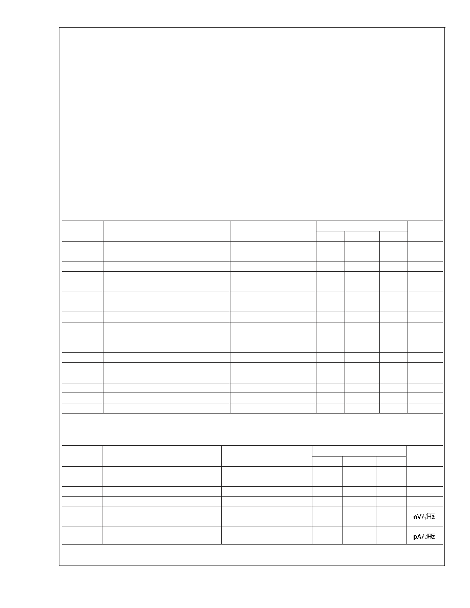
DC Electrical Characteristics
(Note 5)
Symbol
Parameter
Conditions
LF353
Units
MIn
Typ
Max
V
OS
Input Offset Voltage
R
S
=10k
, T
A
=25�C
5
10
mV
Over Temperature
13
mV
V
OS
/
T
Average TC of Input Offset Voltage
R
S
=10 k
10
�V/�C
I
OS
Input Offset Current
T
j
=25�C, (Notes 5, 6)
25
100
pA
T
j
70�C
4
nA
I
B
Input Bias Current
T
j
=25�C, (Notes 5, 6)
50
200
pA
T
j
70�C
8
nA
R
IN
Input Resistance
T
j
=25�C
10
12
A
VOL
Large Signal Voltage Gain
V
S
=
�
15V, T
A
=25�C
25
100
V/mV
V
O
=
�
10V, R
L
=2 k
Over Temperature
15
V/mV
V
O
Output Voltage Swing
V
S
=
�
15V, R
L
=10k
�
12
�
13.5
V
V
CM
Input Common-Mode Voltage
V
S
=
�
15V
�
11
+15
V
Range
-12
V
CMRR
Common-Mode Rejection Ratio
R
S
10k
70
100
dB
PSRR
Supply Voltage Rejection Ratio
(Note 7)
70
100
dB
I
S
Supply Current
3.6
6.5
mA
AC Electrical Characteristics
(Note 5)
Symbol
Parameter
Conditions
LF353
Units
Min
Typ
Max
Amplifier to Amplifier Coupling
T
A
=25�C, f=1 Hz-20 kHz
-120
dB
(Input Referred)
SR
Slew Rate
V
S
=
�
15V, T
A
=25�C
8.0
13
V/�s
GBW
Gain Bandwidth Product
V
S
=
�
15V, T
A
=25�C
2.7
4
MHz
e
n
Equivalent Input Noise Voltage
T
A
=25�C, R
S
=100
,
16
f=1000 Hz
i
n
Equivalent Input Noise Current
T
j
=25�C, f=1000 Hz
0.01
LF353
www.national.com
2
AC Electrical Characteristics
(Continued)
(Note 5)
Symbol
Parameter
Conditions
LF353
Units
Min
Typ
Max
THD
Total Harmonic Distortion
A
V
=+10, RL=10k,
V
O
=20Vp-p,
BW=20 Hz-20 kHz
<
0.02
%
Note 2: For operating at elevated temperatures, the device must be derated based on a thermal resistance of 115�C/W typ junction to ambient for the N package,
and 158�C/W typ junction to ambient for the H package.
Note 3: Unless otherwise specified the absolute maximum negative input voltage is equal to the negative power supply voltage.
Note 4: The power dissipation limit, however, cannot be exceeded.
Note 5: These specifications apply for V
S
=
�
15V and 0�C
T
A
+70�C. V
OS
, I
B
and I
OS
are measured at V
CM
=0.
Note 6: The input bias currents are junction leakage currents which approximately double for every 10�C increase in the junction temperature, T
j
. Due to the limited
production test time, the input bias currents measured are correlated to junction temperature. In normal operation the junction temperature rises above the ambient
temperature as a result of internal power dissipation, P
D
. T
j
=T
A
+
jA
P
D
where
jA
is the thermal resistance from junction to ambient. Use of a heat sink is
recommended if input bias current is to be kept to a minimum.
Note 7: Supply voltage rejection ratio is measured for both supply magnitudes increasing or decreasing simultaneously in accordance with common practice. V
S
=
�
6V to
�
15V.
Note 8: Human body model, 1.5 k
in series with 100 pF.
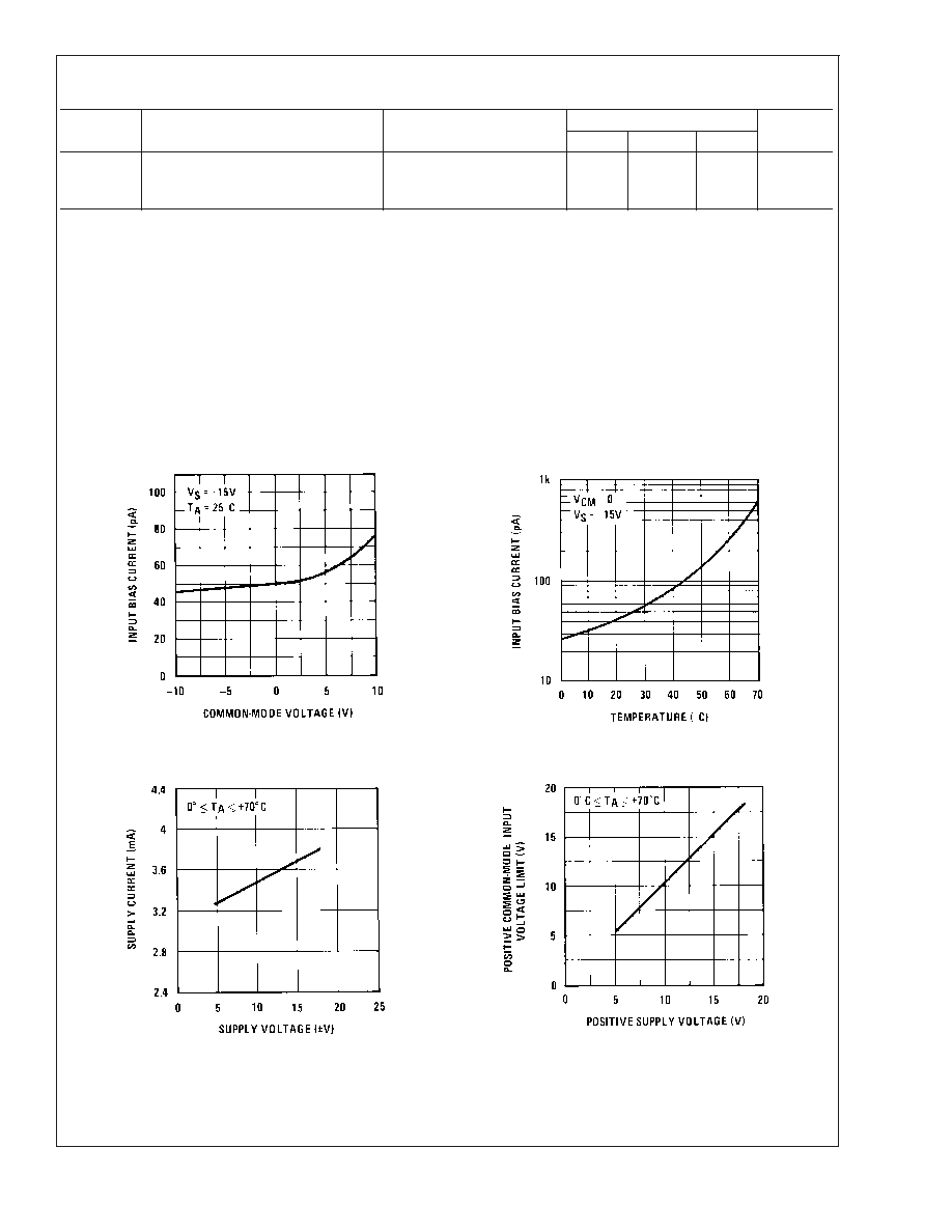
Typical Performance Characteristics
Input Bias Current
Input Bias Current
00564918
00564919
Supply Current
Positive Common-Mode Input Voltage Limit
00564920
00564921
LF353
www.national.com
3
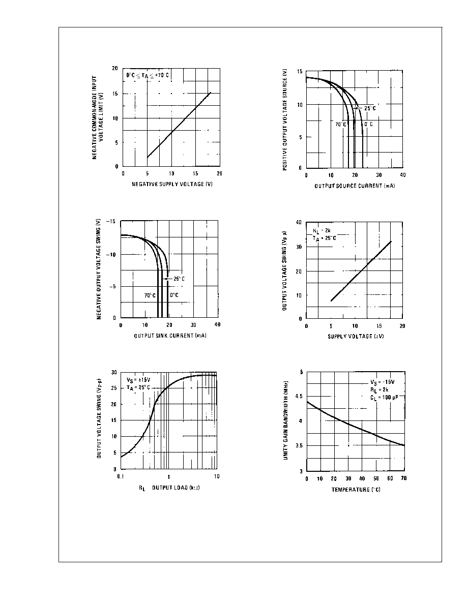
Typical Performance Characteristics
(Continued)
Negative Common-Mode Input Voltage Limit
Positive Current Limit
00564922
00564923
Negative Current Limit
Voltage Swing
00564924
00564925
Output Voltage Swing
Gain Bandwidth
00564926
00564927
LF353
www.national.com
4
Typical Performance Characteristics
(Continued)
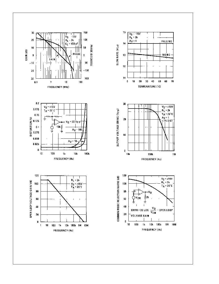
Bode Plot
Slew Rate
00564928
00564929
Distortion vs. Frequency
Undistorted Output Voltage Swing
00564930
00564931
Open Loop Frequency Response
Common-Mode Rejection Ratio
00564932
00564933
LF353
www.national.com
5